Shielded electronic components and method of manufacturing the same
Inactive Publication Date: 2010-07-08
RENESAS ELECTRONICS CORP
View PDF1 Cites 57 Cited by
Summary
Abstract
Description
Claims
Application Information
AI Technical Summary
This helps you quickly interpret patents by identifying the three key elements:
Problems solved by technology
Method used
Benefits of technology
Benefits of technology
[0028]It is supposed that a ratio of metal bonding surface area and a ratio of contact surface area of the shielding metal that is electrically connected with the electrode and the ground wiring connected with a side and / or a surface of the module board are decreased due to deterioration by the temperature cycle test.
[0031]Meanwhile, empirically, a hole in, e.g., a slit-like shape in a shield allows electromagnetic noise to pass through. A slit-like crack generated by deterioration depending on usage environment causes reduction of the shielding effect even when it is short.
[0039]By forming the layer, the anchor effect of the non-electrolytic Ni plating to the resin thereafter can be further stronger. The non-electrolytic Ni plating may be done by a normal method or a non-electrolytic Ni plating method having Ni dissolved in high-pressure CO2 in the same manner with the Pd treatment. The latter method forms a film which forms more diffusion layer because the plating solution itself permeates inside the mold resin.
[0046]Accordingly, a preferred aim of the present invention is to provide an electronic component having a shield with a high reliability in reflow resistance on one side thereof by forming a plating film having no infiltration of CO2 from side surfaces of a board, a high migration reliability, and significantly improved adhesiveness by forming a plating base under high-pressure CO2.
[0051]That is, an advantage obtained by the typical one of the inventions is to manufacture an electronic component having a shield with a high reliability in reflow resistance on one side thereof by forming a plating film having no infiltration of CO2 from side surfaces of a board, a high migration reliability, and significantly improved adhesiveness by forming a plating base under high-pressure CO2.
Problems solved by technology
Also, in a temperature cycle test (e.g., −30° C. / 125° C. in 30 min. cycle) after a reflow test in order to proving reliability, a failure occurs such that the shielding film formed by applying a paste has a deteriorated shielding property as the adhesiveness with the layer connected with the ground is decreased.
Method used
Image
Click on the blue label to locate the original text in one second.
Reading with bidirectional positioning of images and text.
Examples
first embodiment
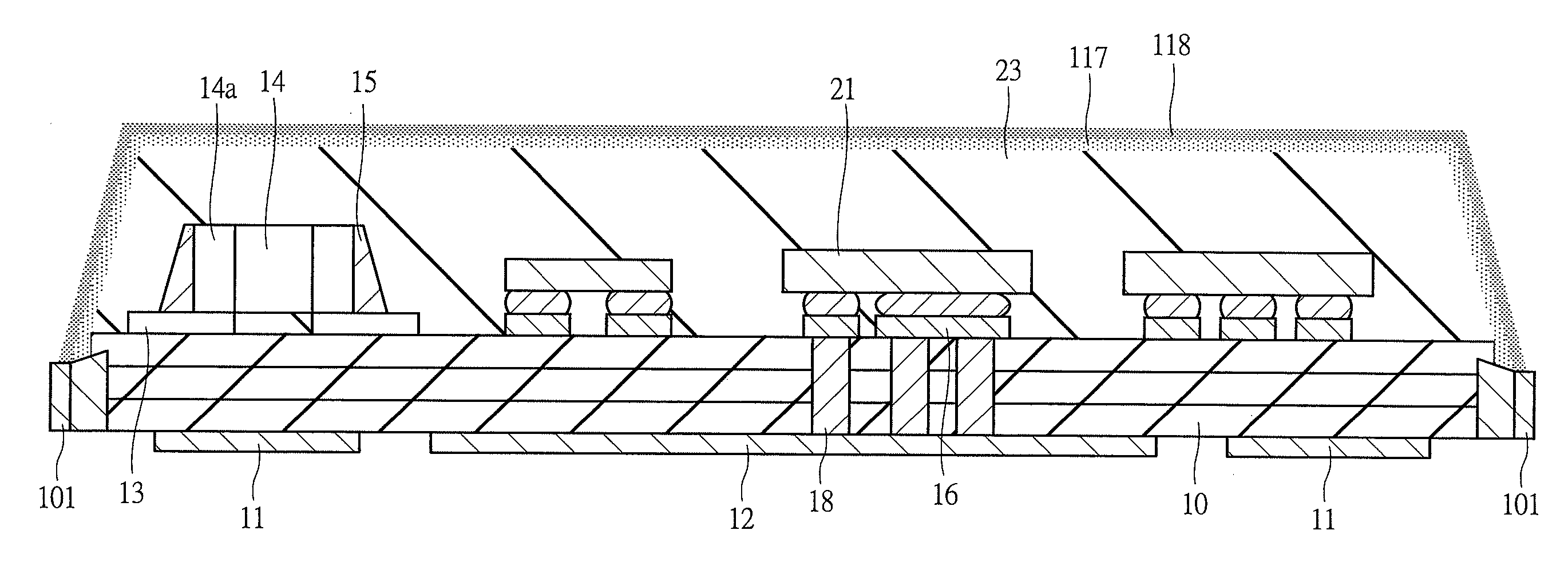
[0069]With reference to FIG. 1, a structure of a shielded electronic component according to a first embodiment of the present invention will be described. FIG. 1 is a cross-sectional view illustrating the structure of the shielded electronic component according to the first embodiment of the present invention and illustrating a structure of a power amplifier module.
[0070]In FIG. 1, a power amplifier module which is the shielded electronic component includes, when the external structure is viewed, a rectangular wiring board 10, a sealant 23 formed with overlapping on a surface (main surface) of the wiring board 10, a plurality of wirings 11 provided to a back surface of the wiring board 10, and a GND (ground) external wiring 12.
[0071]In addition, the sealant 23 is shielded by a Pd pretreatment layer 117 of a Pd complex and a Ni plating film 118. To edge portions of the wiring board 10, GND connection through-holes 101 for a GND wiring layer (not illustrated) or a shield connected to ...
second embodiment
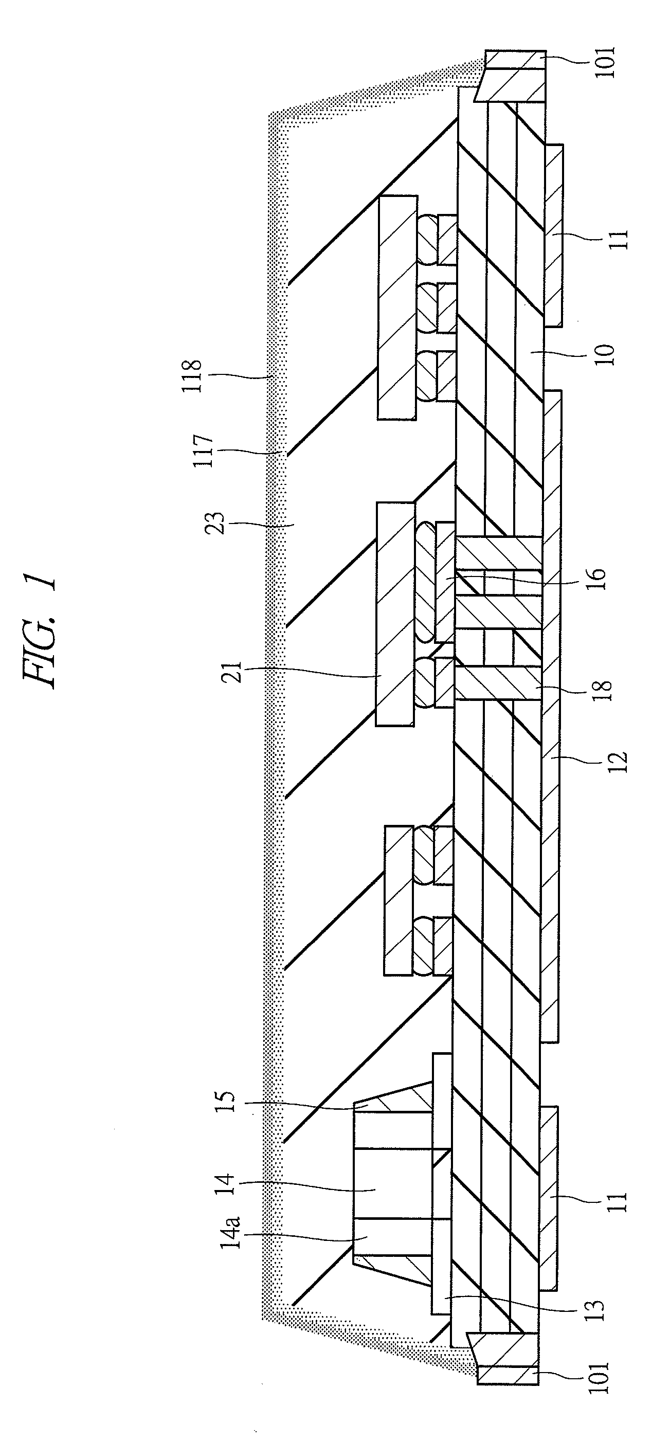
[0091]A shielded electronic component according to a second embodiment has the semiconductor chip 21 of the first embodiment mounted by face-up mounting.
[0092]With reference to FIG. 10, a structure of a shielded electronic component according to the second embodiment of the present invention will be described. FIG. 10 is a cross-sectional view illustrating a structure of the shielded electronic component according to the second embodiment of the present invention, and illustrates a structure of a power amplifier module.
[0093]In FIG. 10, a wiring 13 is formed to a surface of a wiring board 10 in the power amplifier module, and a chip component 14 is formed to be connected to the wiring 13. The chip component 14 is configured by a passive component such as a resistor or capacitor, and an electrode 14a of the chip component 14 and the wiring 13 formed to the wiring board 10 are electrically connected by a solder 15.
[0094]Also, a wiring 16 is connected to a GND external wiring 12 formed...
third embodiment
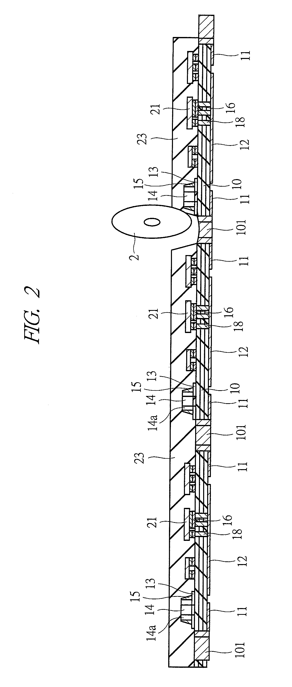
[0099]A shielded electronic component according to a third embodiment has the semiconductor chip 21 formed with a plurality of stacked semiconductors and mounted by face-up mounting.
[0100]With reference to FIG. 11, a structure of the shielded electronic component according to the third embodiment of the present invention will be described. FIG. 11 is a cross-sectional view illustrating the structure of the shielded electronic component according to the third embodiment of the present invention, and illustrating a generally used package. The package is a package of only for a memory, and / or a semiconductor package composed of an ASIC and a memory etc., for example.
[0101]In FIG. 11, the semiconductor chip 21 composed of a plurality of stacked semiconductors attached by a die-attach film 233 having its device forming surface facing upwards (face-up) is stacked on a wiring board 10.
[0102]The semiconductor chip 21 and the wiring board 10 are electrically connected to a wiring 13 on a sur...
PUM
Property
Measurement
Unit
Pressure
aaaaa
aaaaa
Abstract
A shielded electronic component including a wiring board, at least one semiconductorchip mounted on a main surface of the wiring board, a sealant which seals the whole of an upper surface of the wiring board, and a nickel (Ni) plating film formed on an upper surface of the sealant is provided. The Ni plating film is formed on a palladium (Pd) pretreatment layer formed on the upper surface of the sealant with using high-pressure CO2 in a state of protecting a back surface of the wiring board, and is electrically connected with an end portion of a ground wiring layer of the wiring board or a ground (GND) connection through-hole connected with the end portion of the ground wiring layer.
Description
CROSS-REFERENCE TO RELATED APPLICATION[0001]The present application claims priority from Japanese Patent Application No. JP 2008-286254 filed on Nov. 7, 2008, the content of which is hereby incorporated by reference into this application.TECHNICAL FIELD OF THE INVENTION[0002]The present invention relates to a shielded electronic component and a method of manufacturing the same. More particularly, the present invention relates to mounting of electric components including semiconductors such as a semiconductor-mounting electronic component which requires a shielding structure for avoiding adverse effects of ambient radio waves and electromagnetic noise from semiconductors, and a semiconductor mounting electronic component which requires shielding of noise generated from itself.BACKGROUND OF THE INVENTION[0003]A mobile phone will be exemplified to describe a mounting structure of electronic components including semiconductors.[0004]Various electronic components are mounted on a mountin...
Claims
Application Information
Patent Timeline
Application Date:The date an application was filed.
Publication Date:The date a patent or application was officially published.
First Publication Date:The earliest publication date of a patent with the same application number.
Issue Date:Publication date of the patent grant document.
PCT Entry Date:The Entry date of PCT National Phase.
Estimated Expiry Date:The statutory expiry date of a patent right according to the Patent Law, and it is the longest term of protection that the patent right can achieve without the termination of the patent right due to other reasons(Term extension factor has been taken into account ).
Invalid Date:Actual expiry date is based on effective date or publication date of legal transaction data of invalid patent.

