Polysilicon plug bipolar transistor for phase change memory

a phase change memory and polysilicon plug technology, applied in semiconductor devices, digital storage, instruments, etc., can solve the problems of high complexity of design and manufacturing processes, inability to obtain the necessary current,

Active Publication Date: 2010-07-15
TAIWAN SEMICON MFG CO LTD +1
View PDF99 Cites 14 Cited by
  • Summary
  • Abstract
  • Description
  • Claims
  • Application Information

AI Technical Summary

Benefits of technology

[0010]It is therefore desirable to provide phase change memory cells with bipolar junction transistor access devices compatible with CMOS peripheral circuitry while also addressing the complexity of design integration and manufacturing processes.

Problems solved by technology

Issues have arisen in obtaining the necessary current for phase change memory cells having field effect transistor access devices due to the relatively low current drive of field effect transistors.
Bipolar junction transistors can provide larger current drive than field effect transistors, but the integration of bipolar junction transistors with CMOS peripheral circuitry is difficult and results in highly complex designs and manufacturing processes.

Method used


Image

  • Polysilicon plug bipolar transistor for phase change memory
  • Polysilicon plug bipolar transistor for phase change memory
  • Polysilicon plug bipolar transistor for phase change memory

Examples


second embodiment

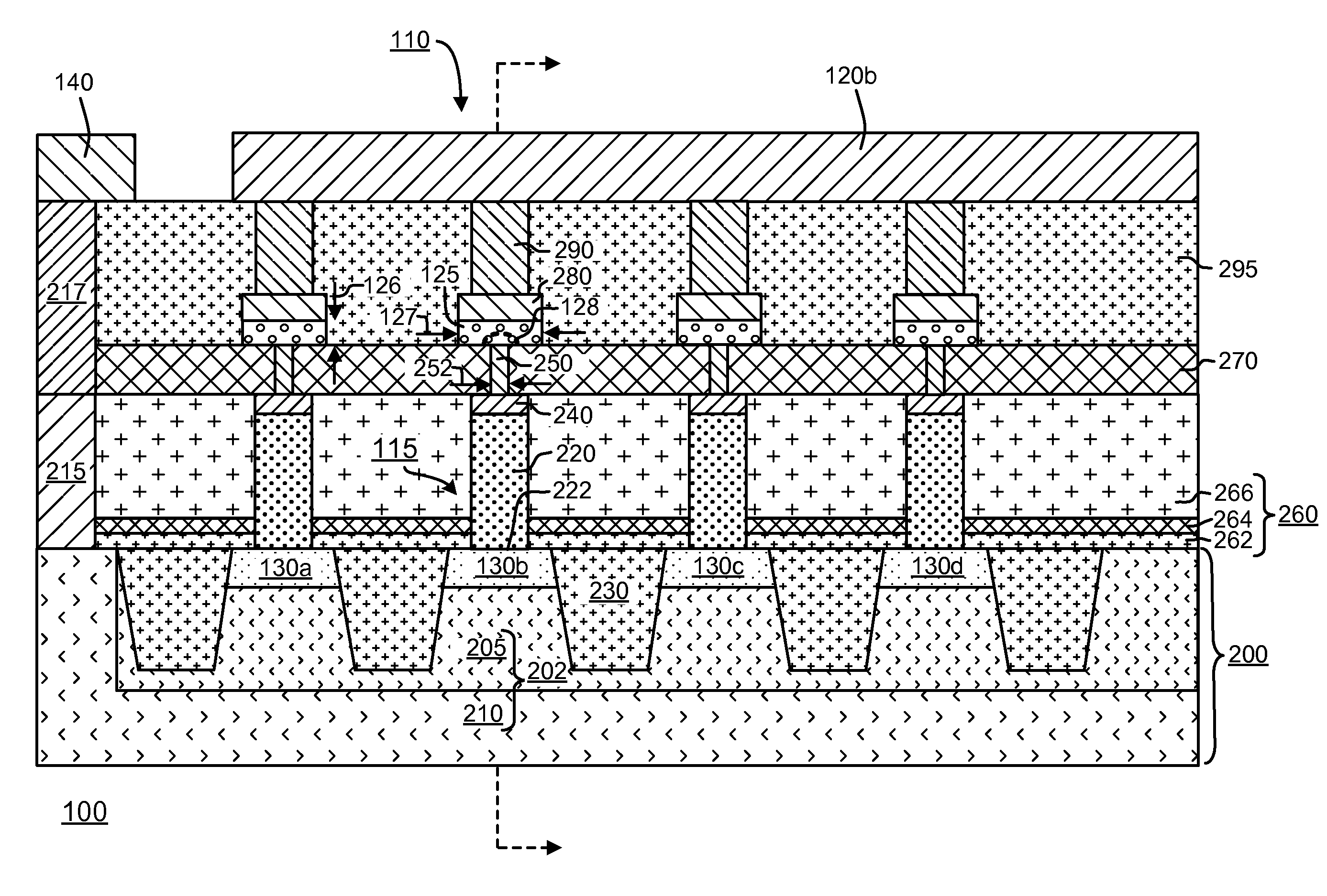
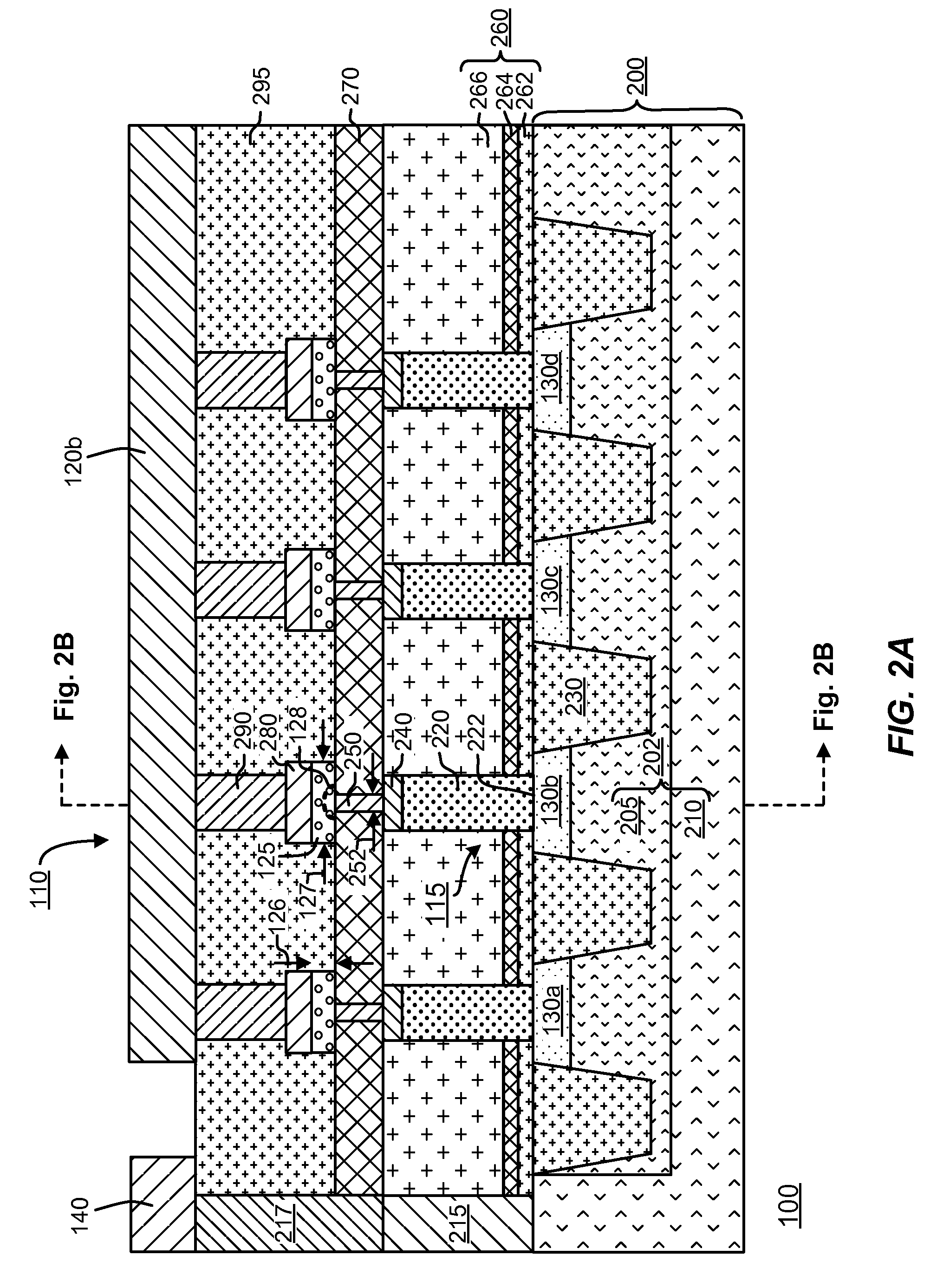
[0051]FIGS. 3A and 3B illustrate cross-sectional views of a portion of memory cells (including representative memory cell 110) arranged in the array 100, FIG. 3A taken along the bit lines 120 and FIG. 3B taken along the word lines 130.

[0052]In the embodiment of FIGS. 3A and 3B the memory element 125 comprises a first portion 323 extending through dielectric layer 270 to contact the conductive cap 240, the first portion 123 being surrounded by the dielectric layer 270. The memory element 125 also includes a second portion 324 on the first portion 323. The memory element 125 couples the conductive cap 240 to the top electrode 280.

[0053]As can be appreciated, the active region 128 can be made extremely small in the illustrated structure, thus reducing the magnitude of the current needed to induce a phase change. The width 300 of the first portion 323 of the memory element 125 is less than that of the conductive cap 240 and the second portion 324 of the memory element 125, and preferabl...

third embodiment

[0054]FIGS. 4A and 4B illustrate cross-sectional views of a portion of memory cells (including representative memory cell 110) arranged in the array 100, FIG. 4A taken along the bit lines 120 and FIG. 4B taken along the word lines 130.

[0055]In the embodiment of FIGS. 4A and 4B the memory element 125 comprises a pillar of memory material extending through dielectric 270 to couple the conductive cap to the top electrode 280, the dielectric 270 surrounding the memory element 125.

[0056]As can be appreciated, the active region 128 can be made extremely small in the illustrated structure, thus reducing the magnitude of the current needed to induce a phase change. The width 400 of the memory element 125 is less than that of the conductive cap 240 and the top electrode 280, and preferably less than a minimum feature size for a process, typically a lithographic process, used to form the array 100.

[0057]This difference in width concentrates current in the small pillar shaped memory element 12...

fourth embodiment

[0058]FIGS. 5A and 5B illustrate cross-sectional views of a portion of memory cells (including representative memory cell 110) arranged in the array 100, FIG. 5A taken along the bit lines 120 and FIG. 5B taken along the word lines 130.

[0059]The embodiment of FIGS. 5A and 5B is similar to the embodiment of FIGS. 2A-2C, with sidewall conductors 510 on the sidewall surfaces of the word lines 130. In the illustrated embodiment the sidewall conductors 510 comprise a self-aligned silicide (salicide) containing, for example, Ti, W, Co, Ni, or Ta. The sidewall conductors 510 increase the electrical conductivity of the word lines 130 and thus reduce the loading of the word lines and improves the uniformity of the array.

[0060]Embodiments of the memory cells described herein include phase change based memory materials, including chalcogenide based materials and other materials, for the memory element. Chalcogens include any of the four elements oxygen (O), sulfur (S), selenium (Se), and tellur...


PUM


Abstract

Memory devices and methods for manufacturing are described herein. A memory device described herein includes a plurality of memory cells. Memory cells in the plurality of memory cells comprise respective bipolar junction transistors and memory elements. The bipolar junction transistors are arranged in a common collector configuration and include an emitter comprising doped polysilicon having a first conductivity type, the emitter contacting a corresponding word line in a plurality of word lines to define a pn junction. The bipolar junction transistors include a portion of the corresponding word line underlying the emitter acting as a base, and a collector comprising a portion of the single-crystalline substrate underlying the base.

Description

CROSS-REFERENCE TO RELATED APPLICATIONS[0001]This application is related to co-pending U.S. patent application Ser. No. ______ entitled “Polysilicon Plug Bipolar Transistor with Self-Aligned Memory Element”, filed on ______ (Attorney Docket No. MXIC 1859-1).PARTIES TO A JOINT RESEARCH AGREEMENT[0002]International Business Machines Corporation, a New York corporation, and Macronix International Corporation, Ltd., a Taiwan corporation, are parties to a Joint Research Agreement.BACKGROUND OF THE INVENTION[0003]1. Field of the Invention[0004]The present invention relates to high density memory devices based on phase change based memory materials, including chalcogenide based materials and on other programmable resistive materials, and methods for manufacturing such devices.[0005]2. Description of Related Art[0006]Phase change based memory materials, like chalcogenide based materials and similar materials, can be caused to change phase between an amorphous state and a crystalline state b...

Claims


Application Information

Patent Timeline
Patent Type & Authority Applications(United States)
IPC IPC(8): H01L29/73H01L47/00H01L21/8222H01L21/8229
CPCG11C13/0004H01L45/1683H01L27/2445H01L27/2463H01L45/04H01L45/06H01L45/085H01L45/1233H01L45/142H01L45/144H01L45/146H01L45/1625H01L45/1641H01L45/1675H01L27/1026
Inventor LUNG, HSIANG-LANLAI, ERH-KUNRAJENDRAN, BIPINLAM, CHUNG H.
Owner TAIWAN SEMICON MFG CO LTD
Why Eureka
Try Eureka