

Solid-state imaging device and electronic apparatus
a solid-state imaging and electronic equipment technology, applied in the direction of radio frequency controlled devices, television system scanning details, television systems, etc., can solve the problems of reducing sensitivity and reducing the aperture area of light receiving portions, so as to reduce the area of column signal processing circuits, reduce the number of pixel transistors per pixel, increase the aperture area of each photodiod
- Summary
- Abstract
- Description
- Claims
- Application Information
AI Technical Summary
Benefits of technology
Problems solved by technology
Method used
Image

Examples
embodiment 1
Exemplary Configuration of Solid-State Imaging Device
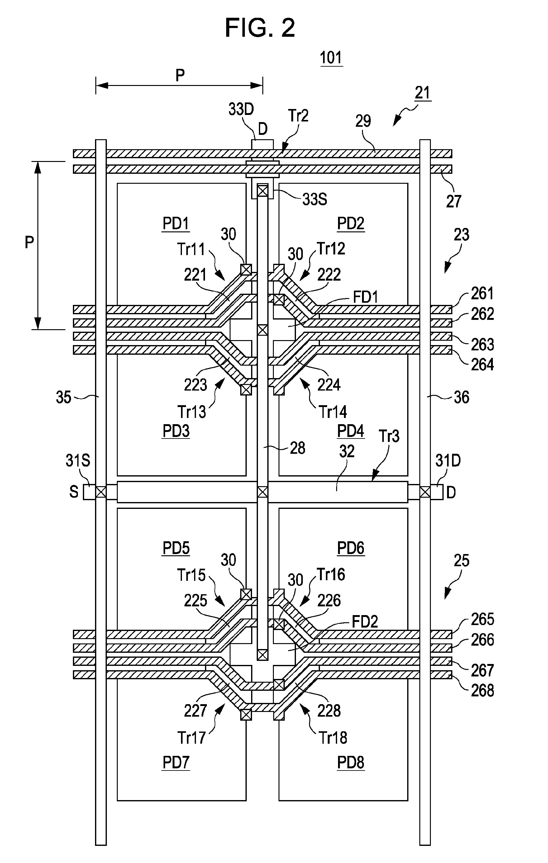
[0085]With reference to FIG. 2, a solid-state imaging device, namely an MOS solid-state imaging device, according to Embodiment 1 of the present invention is illustrated. FIG. 2 illustrates a main part of a layout of a pixel portion. FIGS. 3A to 3C and FIGS. 4 and 5 are exploded planar views for understanding the patterns of first-layer wirings and second-layer wirings. In the following description, a lengthwise or longitudinal direction corresponds to a vertical direction of a pixel portion, and a widthwise or transverse direction corresponds to a horizontal direction of a pixel portion. That is to say, a direction parallel to the vertical signal line is the vertical direction, and a direction vertical to this direction is the horizontal direction.
[0086]As illustrated in FIG. 2, a solid-state imaging device 101 according to Embodiment 1 includes a pixel portion 3 in which sharing units 21 are arranged in a two-dimensional array, ...
embodiment 2
Exemplary Configuration of Solid-State Imaging Device
[0123]With reference to FIG. 6, a solid-state imaging device, namely an MOS solid-state imaging device, according to Embodiment 2 of the present invention is illustrated. FIG. 6 illustrates only the layout of a first-layer metal when the first-layer metal wirings M1 are formed. A solid-state imaging device 102 according to Embodiment 2 includes light shielding portions 45 which are provided for each sharing unit 21 and which are formed by the first-layer metal on each of the floating diffusions FD1 and FD2. That is to say, in the solid-state imaging device, 102 the readout wirings 261 to 268, the reset wiring 27, the power supply wiring 29 that is connected to the drain region of the reset transistor Tr2 are formed by the first-layer metal wirings M1. Moreover, the light shielding portions 45 are formed by the first-layer metal wirings M1 so as to cover the floating diffusions FD1 and FD2. Since other configurations are the same a...
embodiment 3
Exemplary Configuration of Solid-State Imaging Device
[0130]With reference to FIGS. 9 and 10, a solid-state imaging device, namely an MOS solid-state imaging device, according to Embodiment 3 of the present invention is illustrated. FIG. 9 illustrates a main part of a layout of a pixel portion. FIG. 10 illustrates the pattern of the first-layer wirings. A solid-state imaging device 103 according to Embodiment 3 has one sharing unit 21 in which at least one of the readout wirings in unit pixels is disposed within the regions of the photodiodes PD, and the regions of the photodiodes PD are disposed on both sides of and right below the one readout wiring.
[0131]In this example, in one sharing unit 21, among a plurality of readout wirings on the same layer which are disposed within the pixel pitch P, one readout wiring is spaced apart from the other readout wirings. This readout wiring is disposed at a distance d2 from the other readout wirings, wherein the distance d2 is larger than a mi...
PUM
 Abstract
Description
Claims
Application Information