

Semiconductor device
a technology of semiconductor devices and semiconductors, applied in semiconductor devices, semiconductor/solid-state device details, electrical apparatus, etc., can solve the problems of reducing the joint strength between the bonding wire and the leadframe, affecting the manufacturing cost and mass production of the leadframe, and affecting the effect of ultrasonic damping on the bonding wire join
- Summary
- Abstract
- Description
- Claims
- Application Information
AI Technical Summary
Benefits of technology
Problems solved by technology
Method used
Image

Examples
first embodiment
[0044]A first embodiment is used for manufacture of a power MOSFET package, and will be described with reference to FIGS. 2 to 6.
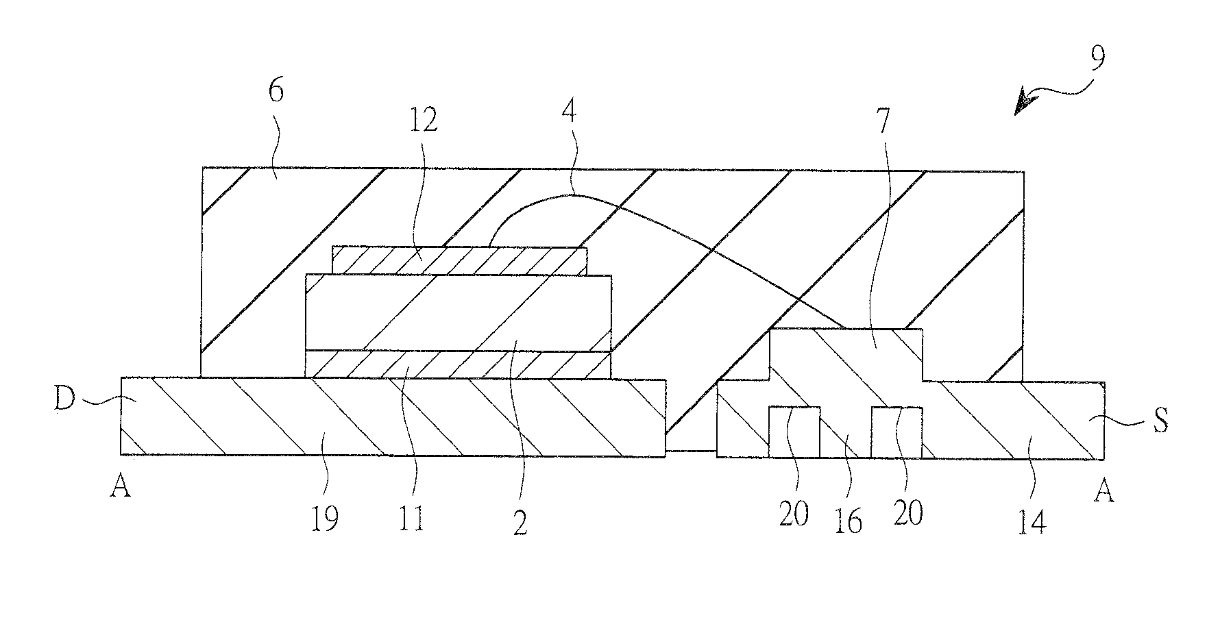
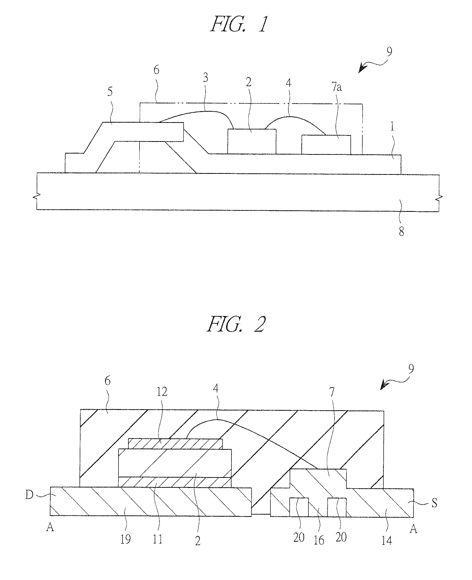
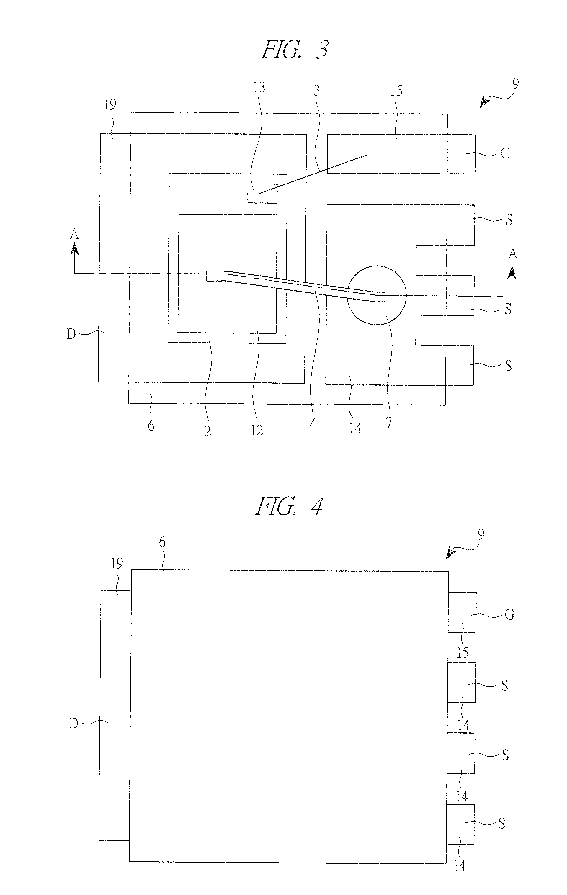
[0045]FIG. 2 is a cross-sectional view taken along the line A-A in FIG. 3, and illustrates an internal structure of a semiconductor device 9 according to the present embodiment. FIG. 3 is a plan view illustrating the internal structure of the semiconductor device 9 of FIG. 2, and an outline of a resin 6 is illustrated by a two-dot chain line. Also, FIGS. 4 and 5 illustrate appearance configurations of the semiconductor device 9 according to the present embodiment. FIG. 4 is a top plan view of the semiconductor device 9, and FIG. 5 is a bottom plan view of the same.
[0046]The present embodiment is an example of using the present invention for a vertical power transistor. That is, a field effect transistor having a drain electrode “D”, a source electrode “S”, and a gate electrode “G” is embedded in a semiconductor chip 2, and the semiconductor chip 2 is embed...
second embodiment
[0058]A second embodiment is used for manufacture of a power MOSFET package, and will be described with reference to FIGS. 7 to 10.
[0059]FIG. 7 is a cross-sectional view taken along the line B-B in FIG. 8, and illustrates an internal structure of a semiconductor device 9 according to the present embodiment. FIG. 8 is a plan view illustrating the internal structure of the semiconductor device 9 of FIG. 7, and an outline of a resin 6 is illustrated by a two-dot chain line. Also, FIGS. 9 and 10 illustrate appearance configurations of the semiconductor device 9 according to the present embodiment. FIG. 9 is a top plan view of the semiconductor device 9, and FIG. 10 is a bottom plan view of the same.
[0060]As illustrated in FIG. 7, the semiconductor device 9 according to the present embodiment has a bump 17 in a periphery of the bonding portion of the boss 7 in the semiconductor device 9 according to the first embodiment so as to continuously surround the bonding portion.
[0061]In the semi...
third embodiment
[0065]A third embodiment is used for manufacture of a power-MOSFET package, and will be described with reference to FIGS. 11 to 14.
[0066]FIG. 11 is a cross-sectional view taken along the line C-C in FIG. 12, and illustrates an internal structure of a semiconductor device 9 according to the present embodiment. FIG. 12 is a plan view illustrating the internal structure of the semiconductor device 9 of FIG. 11, and an outline of a resin 6 is illustrated by a two-dot chain line. Also, FIGS. 13 and 14 illustrate appearance configurations of the semiconductor device 9 according to the present embodiment. FIG. 13 is a top plan view of the semiconductor device 9, and FIG. 14 is a bottom plan view of the same.
[0067]The semiconductor device 9 according to the present embodiment has a peripheral boss 18 on a periphery of the bonding portion so as to continuously surround the bonding portion instead of the boss 7 and the support pillar 16 in the semiconductor device 9 according to the first emb...
PUM
 Abstract
Description
Claims
Application Information