Display element, image display device, and image display system

a display element and image technology, applied in the field of display elements, can solve the problems of reducing the thickness of the cell wall separating adjacent cells, reducing display properties such as lower reflectance and contrast, and reducing the thickness of the bottom wall of the cells, so as to achieve the effect of improving display properties and strength, reducing the thickness of the cell wall, and sufficient strength

Inactive Publication Date: 2010-07-29
RICOH KK
View PDF7 Cites 16 Cited by
  • Summary
  • Abstract
  • Description
  • Claims
  • Application Information

AI Technical Summary

Benefits of technology

[0052]A display element having the characteristic (2) is described below with reference to the hollow structure 20 (a sheet having a honeycomb structure) of FIG. 3. The thickness of each of the upper wall 23 and the lower wall 25 of the hollow structure is in the range of 0.01-10 μm, and preferably in the range of 0.05-5 μm. With this configuration, the display element including the hollow structure 20 can provide improved display properties. The upper wall 23 and the lower wall 25 with such reduced thicknesses provide advantageous effects in terms of reflectance and drive voltage. If the thickness of the upper wall 23 and the lower wall 25 is less than 0.01 μm, the strength of the hollow structure 20 is reduced. If the thickness is greater than 10 μm, the properties of the display element are reduced in terms of reflectance and drive voltage.
[0053]A display element having the characteristic (3) is described below with reference to the hollow structure 20 (a sheet having a honeycomb structure) of FIG. 3. In the hollow structure 20, the joint portion 26a and the joint portion 26b have curved cross-sectional shapes, a curvature radius of each of which is in the range of 0.1-50 μm, and preferably in the range of 1-10 μm. With this configuration, the display element including the hollow structure 20 can provide improved display properties and strength. Thus, the display element can exhibit sufficient strength even when bent for use. That is, the provision of the joint portions 26a and 26b having a greater thickness than the cell wall 22 can improve the strength of the display element. If the curvature radius is less than 0.1 μm, the strength of the display element is sufficient to tolerate being slightly bent, but not sufficient to tolerate being rolled up. If the curvature radius is greater than 50 μm, the display properties are reduced, especially in terms of reflectance.
[0054]A display element having the characteristic (4) is described below with reference to the hollow structure 20 (a sheet having a honeycomb structure) of FIG. 3. In the hollow structure 20, a solvent having one or more types of white particles / colored particles dispersed therein is disposed in the cells 21. The openings 24 of the cells 21 are sealed with a resin insoluble in the solvent. The resin with which the openings 24 are sealed is a film, the thickness of which is in the range of 0.1-10 μm, and preferably in the range of 0.5-5 μm. With this configuration, the display element including the hollow structure 20 can provide improved display properties and strength. The resin film with such a reduced thickness provides advantageous effects in terms of reflectance and drive voltage. If the film thickness is less than 0.1 μm, the strength of the hollow structure 20 is reduced. If the film thickness is greater than 10 μm, the properties of the display element are reduced in terms of reflectance and drive voltage.
[0055]According to a second embodiment of the present invention, a display element comprises a hollow structure. The hollow structure includes plural cells disposed in a plane, each having a first opening and a second opening respectively in a first wall and a second wall, opposite to the first wall, of the hollow structure; and a partition wall separating the adjacent cells. A solvent having one or more types of white particles and / or colored particles dispersed therein is disposed in the cells. The first openings in the first wall are sealed with a resin insoluble in the solvent. The display element of the second embodiment has at least one of the following characteristics (5)-(8).
[0056](5) The thickness of the partition wall (cell wall) separating the adjacent cells is in the range of 0.01-10 μm, and preferably in the range of 0.05-5 μm.
[0057](6) The thickness of each of the first wall and the second wall of the hollow structure is in the range of 0.01-10 μm, and preferably in the range of 0.05-5 μm.

Problems solved by technology

A problem with this electrophoresis display is that, because microembossing or imagewise exposure is used for creating the cells, it is difficult to reduce the thickness of the cell wall separating the adjacent cells.
The thicker the cell wall, the smaller the display area, resulting in reduced display properties such as lower reflectance and contrast.
The use of microembossing or imagewise exposure for creating the cells also makes it difficult to reduce the thickness of bottom walls of the cells.
Accordingly, it is difficult to create cells with a bottom wall thickness of 10 μm or less.
With this technique, it is difficult to handle a film with a thickness of 10 μm or less.
Accordingly, it is difficult to create cells with a bottom wall thickness of 10 μm or less.
It is therefore impossible to reduce a drive voltage required for driving the charged pigment particles filling the cells.
The greater the thickness of the polymer sealing film, the lower the reflectance, resulting in requiring high drive voltage.

Method used


Image

  • Display element, image display device, and image display system
  • Display element, image display device, and image display system
  • Display element, image display device, and image display system

Examples


example 1

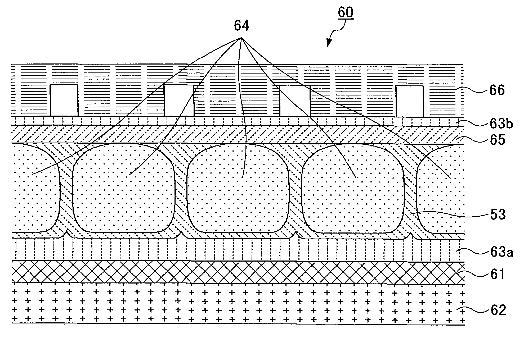
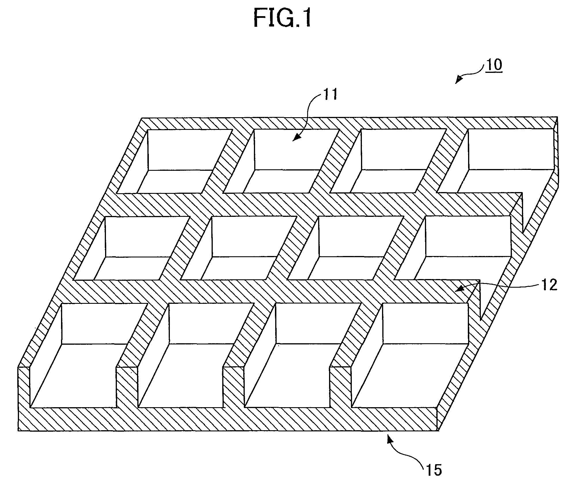
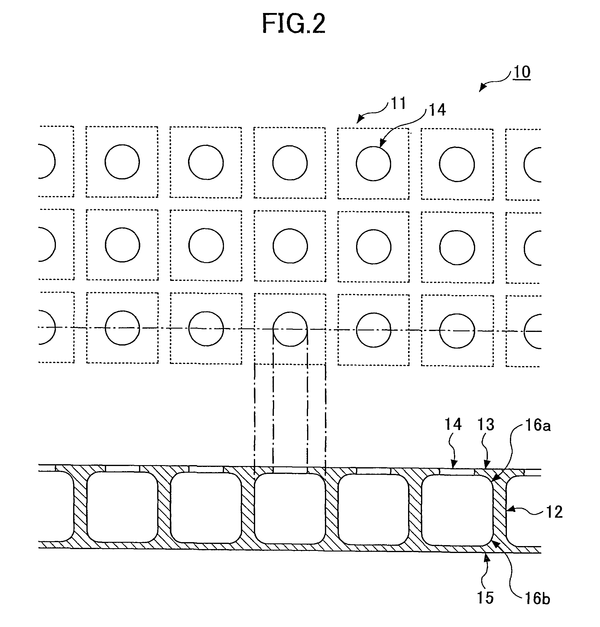
[0087]An image display device 60 shown in FIG. 9 was manufactured. A hollow structure used was one of the hollow structures 53 (see FIGS. 3 and 4) of Manufacture Examples 1-5, which includes plural cells disposed in a plane. Each of the cells has an opening. In the hollow structure 53, the thickness of the cell wall was 2 μm; the thickness of each of the upper and lower walls was 1 μm; the depth of each cell was 50 μm; the cell-to-cell pitch was 150 μm; and joint portions of the upper and lower walls with the cell wall had curved cross-sectional shapes of a 5 μm curvature radius.

[0088]In the image display device 60, the lower wall of the hollow structure 53 is bonded by an adhesive layer 63a to a PET film 62 with an ITO layer 61 formed thereon. An ultraviolet curing adhesive, an epoxy-based adhesive, or other suitable adhesives may be used for bonding. This structure can be obtained by bonding the PET film 62 with the ITO layer 61 formed thereon onto the hollow structure 53 (see FIG...

example 2

[0091]An image display device 70 shown in FIG. 10 was manufactured. A hollow structure used was one of the hollow structures 53 (see FIGS. 3 and 4) of Manufacture Examples 1-5, which includes plural cells disposed in a plane. Each of the cells has an opening. In the hollow structure 53, the thickness of the cell wall was 2 μm; the thickness of each of the upper and lower walls was 1 μm; the depth of each cell was 50 μm; the cell-to-cell pitch was 150 μm; and joint portions of the upper and lower walls with the cell wall had curved cross-sectional shapes of a 5 μm curvature radius.

[0092]In the image display device 70, the lower wall of the hollow structure 53 is bonded by an adhesive layer 63a to a voltage drive circuit 66. An ultraviolet curing adhesive, an epoxy-based adhesive, or other suitable adhesives may be used for bonding. This structure can be obtained by bonding the voltage drive circuit 66 onto the hollow structure 53 (see FIG. 7C) and then separating the hollow structure...

example 3

[0095]An image display device 80 shown in FIG. 11 was manufactured. A hollow structure used was one of the hollow structures 53 (see FIGS. 6 and 4) of Manufacture Examples 1-5, which includes plural cells disposed in a plane. Each cell has opposite openings. In the hollow structure 53, the thickness of the cell wall was 2 μm; the thickness of each of the upper and lower walls was 1 μm; the depth of each cell was 50 μm; the cell-to-cell pitch was 150 μm; and joint portions of the upper and lower walls with the cell wall had curved cross-sectional shapes of a 5 μm curvature radius.

[0096]In the image display device 80, the lower wall of the hollow structure 53 is bonded by an adhesive layer 63a to a voltage drive circuit 66. An ultraviolet curing adhesive, an epoxy-based adhesive, or other suitable adhesives may be used for bonding. This structure can be obtained by bonding the voltage drive circuit 66 onto the hollow structure 53 (see FIG. 7C) and then separating the hollow structure ...


PUM

PropertyMeasurementUnit
thicknessaaaaaaaaaa
thicknessaaaaaaaaaa
curvature radiusaaaaaaaaaa

Abstract

A display element includes a hollow structure. The hollow structure includes plural cells disposed in a plane, each having an opening in a first wall of the hollow structure, and a partition wall separating the adjacent cells. A solvent having one or more types of white particles and / or colored particles dispersed therein is disposed in the cells. The openings are sealed with a resin insoluble in the solvent. A thickness of the partition wall separating the adjacent cells is 0.01 μm or greater but not greater than 10 μm.

Description

TECHNICAL FIELD[0001]The present invention relates to a display element, an image display device, and an image display system.BACKGROUND ART[0002]An electrophoresis display is a non-emissive device based on the electrophoresis phenomenon of charged pigment particles suspended in a solvent. The electrophoresis display usually comprises two plates with electrodes placed opposing each other, separated by using spacers. One of the electrodes is usually transparent. A suspension is enclosed between the two plates. When a voltage difference is imposed between the two electrodes, the pigment particles migrate to one side and then either the color of the pigment or the color of the solvent can be seen according to the polarity of the voltage difference.[0003]PCT International Publication No. WO / 2001 / 067170 discloses an electrophoresis display that includes plural cup-like indentations (cells) created by microembossing or imagewise exposure. The cells are filled with dispersions, which are c...

Claims


Application Information

Patent Timeline
Patent Type & Authority Applications(United States)
IPC IPC(8): G02F1/167G02F1/1679
CPCG02F2001/1672G02F1/167B29D11/00365G02F1/1681G02F1/1679G02F2001/1678
Inventor KANEMATSU, TOSHIHIROOHGAKI, MASARUAOKI, SHINJIOHSHIMA, HISAYOSHISENO, SHINYAMASUZAWA, MASAHIRO
Owner RICOH KK
Why Eureka
Try Eureka