

Ultrasonic probe
- Summary
- Abstract
- Description
- Claims
- Application Information
AI Technical Summary
Benefits of technology
Problems solved by technology
Method used
Image

Examples
first embodiment
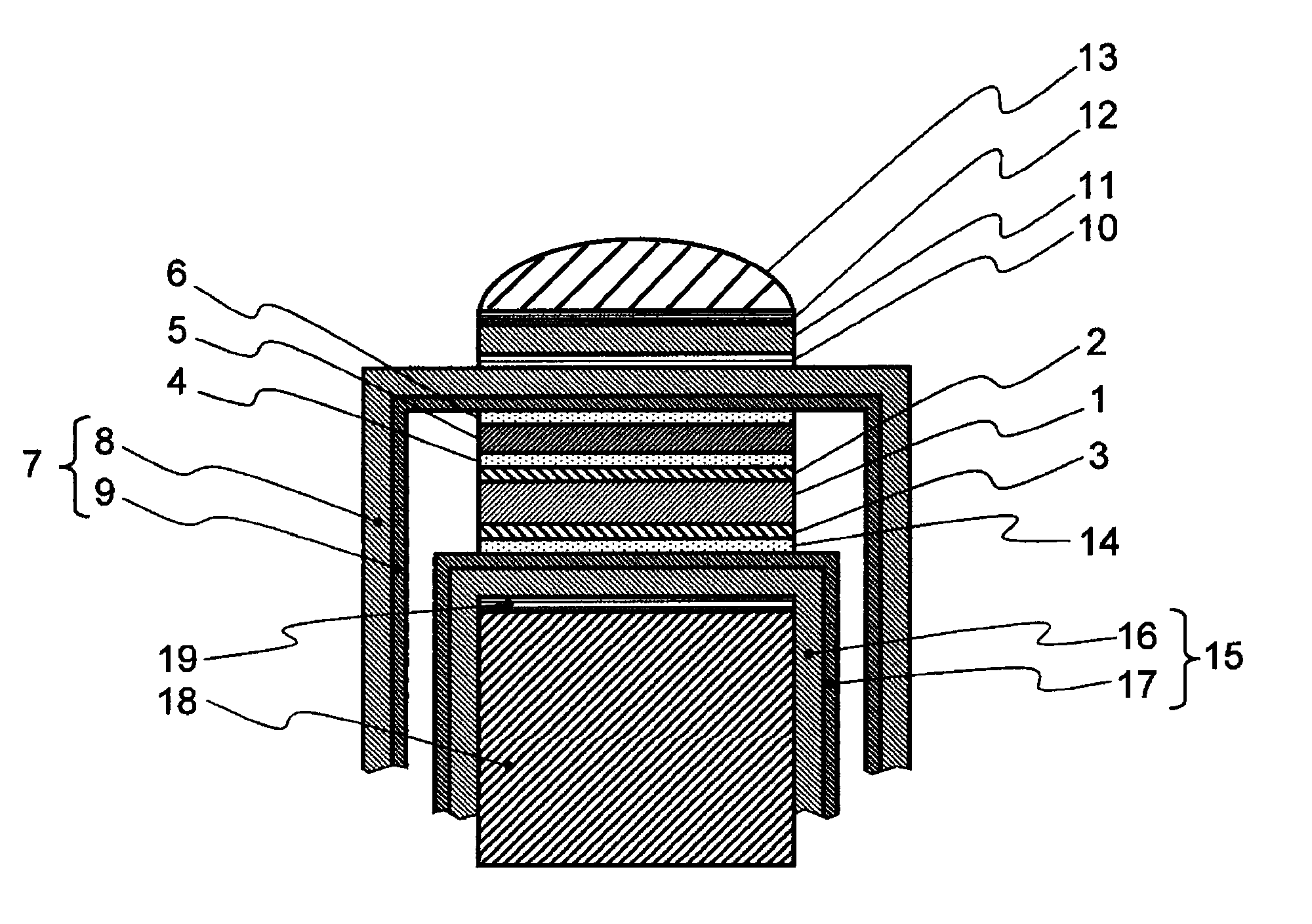
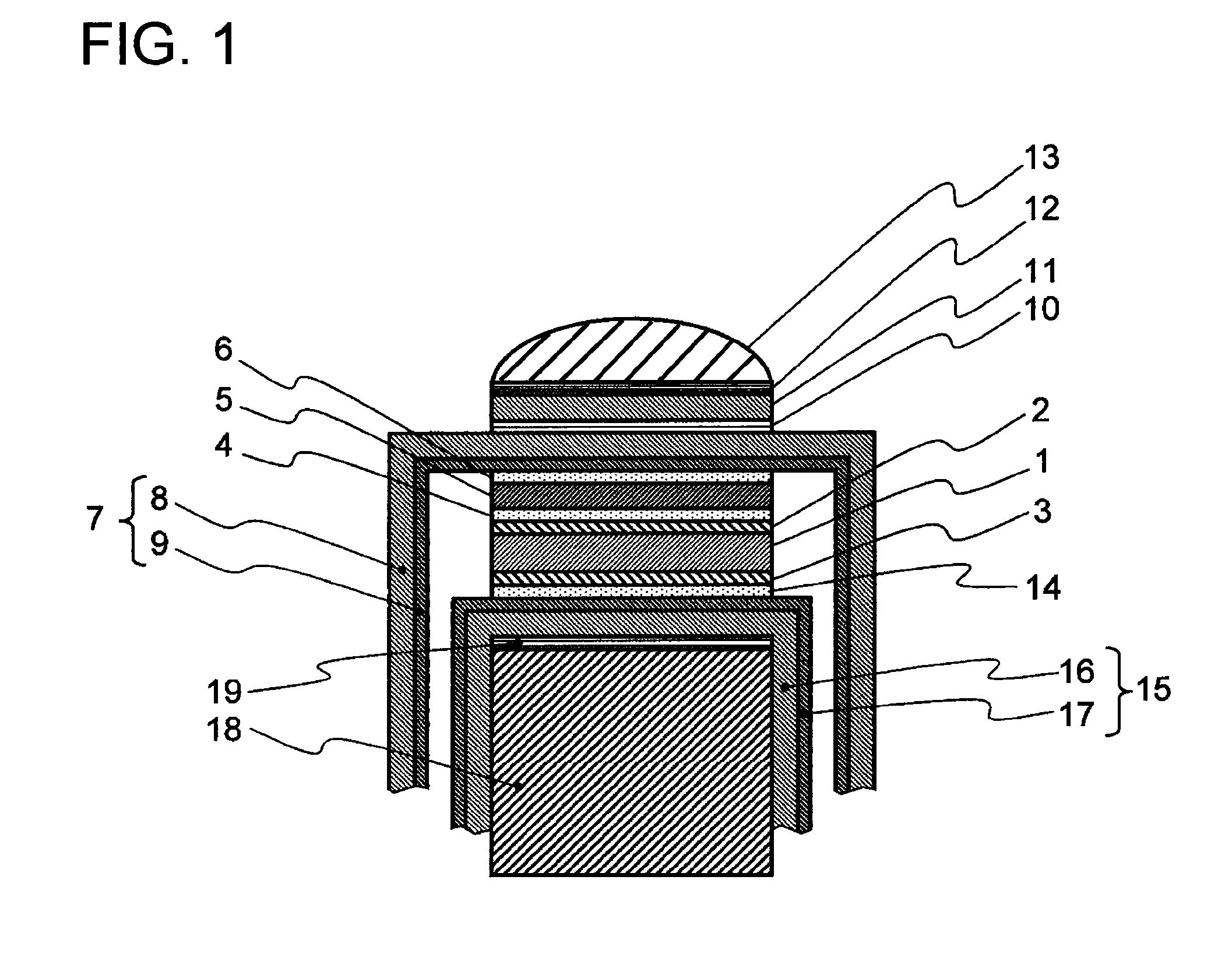
[0040]FIG. 1 shows the ultrasonic probe in the first embodiment according to the present invention. FIG. 1 is the sectional view in the short axis direction of the ultrasonic probe. By the way, in the explanation of this drawing, [UP] and [DOWN] are assumed to indicate the upward direction and the downward direction in the plane of the drawing paper, respectively (similarly also in FIGS. 4 and 6). In FIG. 1, a piezoelectric element 1 is a piezoelectric element in which a piezoelectric ceramics such as a PZT group and the like, a single crystal, and a polymer such as PVDF and the like are used. On one surface of each of a plurality of piezoelectric elements 1, a ground electrode layer 2 is formed as a first electrode layer, and on the other side, a positive electrode layer 3 is formed as a second electrode layer, respectively, in advance.
[0041]In this embodiment, the ground electrode layer 2 and the positive electrode layer 3 are assumed to be the gold sputter electrode layers whose ...
second embodiment
[0064]The ultrasonic probe of the second embodiment according to the present invention will be described below.
[0065]In the ultrasonic probe in the second embodiment, a 10-point average roughness (Rz) on the surfaces of the electrode layers formed on both the surfaces of the piezoelectric element 1 in the ultrasonic probe in the first embodiment is set to a range from 3.5 μm to 6.5 μm. Moreover, an average particle diameter between the graphite powder of the thermosetting two-component type adhesive layers 4, 6 and 14 in which the graphite powder is uniformly distributed to adhere the polymer film 7, the conductive acoustic matching layer 5, the piezoelectric element 1 and the FPC 15, respectively, is set to a range from 3.5 μm to 6.5 μm.
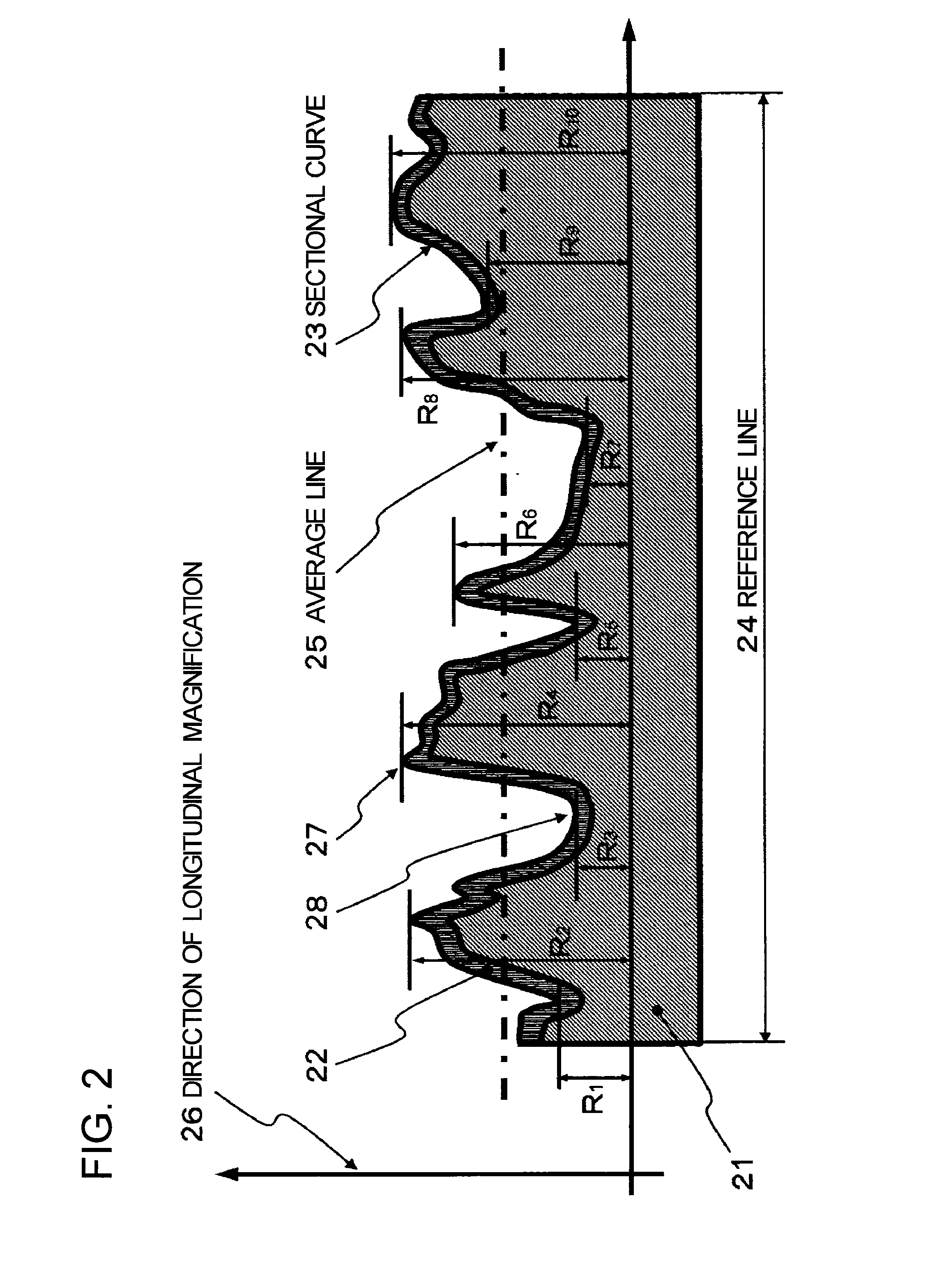
[0066]FIG. 2 shows the shape (the roughness) of the surface on the section of a piezoelectric element 21.
[0067]A ground electrode layer 22 is a layer that is formed on the surface of the piezoelectric element 21 by the gold sputtering (the positive ...
third embodiment
[0081]As mentioned above, according to the ultrasonic probe in the third embodiment according to the present invention, the graphite powder is uniformly distributed in: the adhesive layer 1 that is located between the first electrode layer formed on one side of the piezoelectric element and one or more conductive acoustic matching layers; and the adhesive layer 2 that is located between one or more conductive acoustic matching layers and the first film on which the electrode pattern is formed, and the tungsten powder is uniformly distributed in the adhesive layer 3 that is located between the second electrode layer formed on the other side of the piezoelectric element and the second film on which the electrode pattern is formed. Thus, the reflection loss of the ultrasonic waves generated on the boundary surface between the acoustic media is reduced, which results in the improvement of the sensibility of the ultrasonic probe.
PUM
 Abstract
Description
Claims
Application Information