Data transfer device and data transfer method

a data transfer device and data transfer technology, applied in the direction of digital transmission, generating/distributing signals, instruments, etc., can solve the problems of generating a difference in timing on the entire system, difficult to conduct the action timing verification equivalent to the actual device with bit precision, and using a relatively complicated circuit device, etc., to achieve secure the margin of setup time, increase verification precision, and not deteriorate the effect of data transfer throughpu

Active Publication Date: 2010-08-05
NEC CORP
View PDF6 Cites 17 Cited by
  • Summary
  • Abstract
  • Description
  • Claims
  • Application Information

AI Technical Summary

Benefits of technology

[0015]With the present invention, data is latched as reception data by the delay clock signal. Thus, it is possible to achieve synchronous transfer of data between the LSIs, even when the wiring delay between the LSIs varies on the evaluation board, the actual device, and the like.
[0016]Next, exemplary embodiments of the invention will be described by referring to the drawings.
[0017]A data transfer device according to the exemplary embodiments of the invention is a data transfer device which transfer data with a partner device. As shown in FIG. 1, FIG. 10, FIG. 11, and FIG. 12, as the basic structure, the data transfer device includes: a clock sending section 400 which transmits a transfer clock signal CLK(ExCLK) to a partner device (2); and a data receiving section 500 which receives data MDI from the partner device (2) by synchronizing with the transfer clock signal CLK(ExCLK). The data receiving section 500 includes a first latch circuit 21 which latches the data at a rise edge or a fall edge of a delay clock signal DCLK that is delayed from the transfer clock signal CLK by a variable delay amount, and the output signal of the first latch circuit 21 is processed as the received data.
[0018]In the exemplary embodiment of the invention, in order to synchronize the timings in the entire system, the transfer clock signal CLK(ExCLK) is transferred only to the partner device (2), and data transmission is performed mutually with the partner device (2) by synchronizing in common with the transfer clock signal CLK(ExCLK). Further, regarding the clock frequency of the transfer clock signal CLK(ExCLK), it is desirable to be set to the clock frequency which satisfies the required performance of the actual device so as not to deteriorate the data transfer throughput.
[0019]With the exemplary embodiment of the invention, it is pos

Problems solved by technology

In this case, however, it is necessary to use a relatively complicated circuit device which includes a feedback loop for phase adjustment when the phase of the clock is adjusted on the receiver side.
Further, since there is a difference in wiring delay of the LSIs between an evaluation board and an actual device or the like, there may generate a difference in timings on the entire system (between the LSIs) depending on the wiring delay.
Such difference may generate a case where the entire system cannot be synchronized or a case where it is difficult to conduct the acti

Method used


Image

  • Data transfer device and data transfer method
  • Data transfer device and data transfer method
  • Data transfer device and data transfer method

Examples


first exemplary embodiment

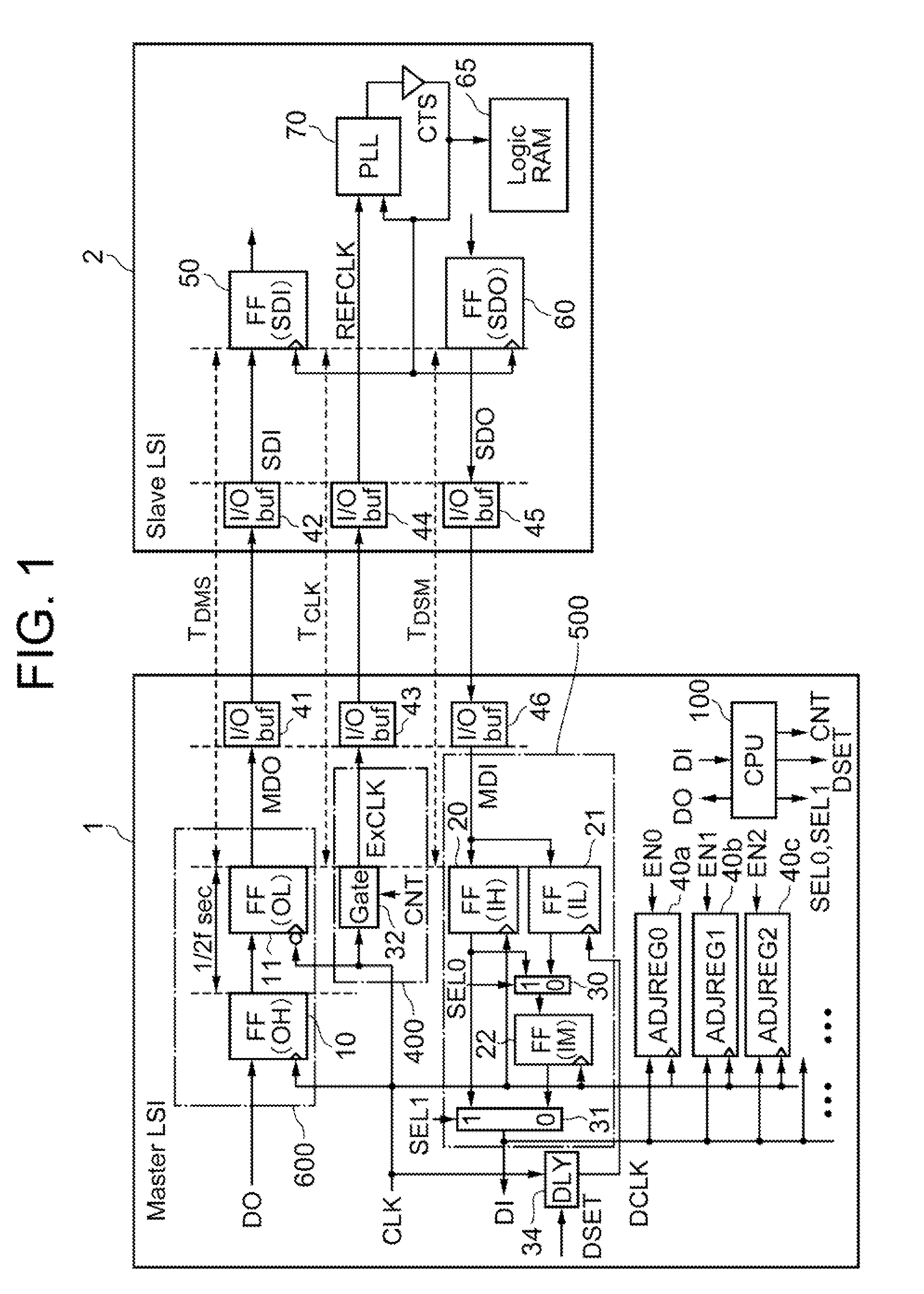
[0022]FIG. 1 is a block diagram showing the structure of the data transfer device according to the first exemplary embodiment of the invention. In following explanations of each of the exemplary embodiments, described is a case where the data transfer device according to the exemplary embodiments of the invention is mounted into the master LSI, and a slave LSI is used as the partner device.

[0023]The master LSI includes: flip-flops 10(FF(OH)), 11(FF(OL)), 20(FF(IH)), 21(FF(IL)), 22(FF(IM)), selecting circuits (selectors) 30, 31, a gate circuit 32, phase adjusting registers 40a(ADJREG0), 40b(ADJREG1), 40c(ADJREG2), - - - , input / output buffers 41, 43, 46, a delay register (DLY) 34, and a control processor (CPU) 100. Further, the slave LSI2 includes input / output buffers 42, 44, 45, flip-flops 50(FF(SDI)), 60(FF(SDO)), a PLL circuit 70, and an internal circuit 65 such as RAM and a logic circuit.

[0024]In the first exemplary embodiment shown in FIG. 1, the gate circuit 32 and the like for...

example 1

[0070]FIG. 9 shows a case where the data transfer device according to the first exemplary embodiment of the invention shown in FIG. 1 is applied to a W-CDMA (Wideband Code Division Multiple Access) digital base band (DBB) LSI system having an HSDPA (High Speed Downlink Packet Access) function expansion which is one of examples of an accelerator expansion system that uses a plurality of LSIs.

[0071]The WCDMA DBB LSI as a master LSI1a is provided with: a processor (CPU) 100a for controlling the entire W-CDMA digital base band LSI system; a clock control circuit 300 (CLK Ctrl); and bus controller circuits 201, 202 (BUSC1, BUSC2) which conduct data transfer with a slave LSI2a. The clock control circuit 300 supplies a clock signal CLK used for transfer and a clock signal DCLK used for phase adjustment to the bus controller circuits 201, 202. Further, the HSDPA DBB LSI as a slave LSI2a is provided with: bus interface circuits 203, 204 (BUSIF1, BUSIF2) which conduct data transfer with the m...

second exemplary embodiment

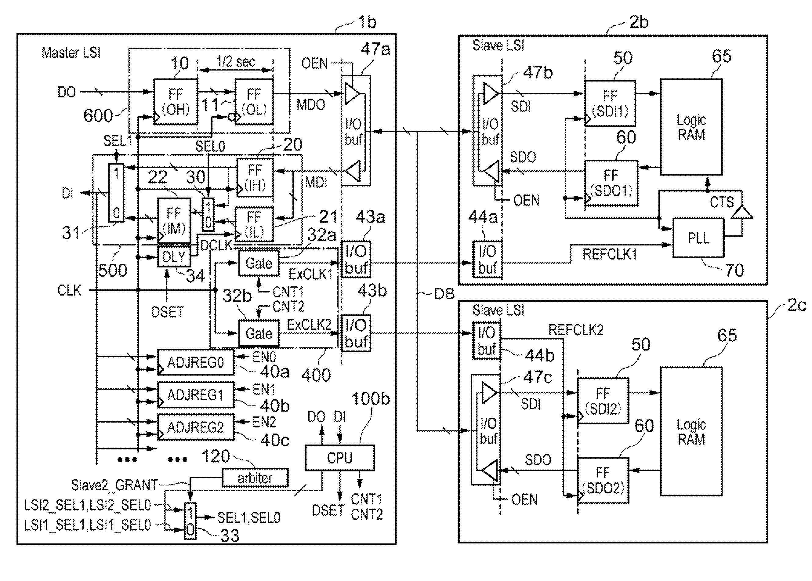
[0074]FIG. 10 is a block diagram showing the structure of a data transfer device according to a second exemplary embodiment of the invention. The second exemplary embodiment shown in FIG. 10 is structured in such a manner that a data output circuit 600 transfers transfer data to a plurality of partner devices 2 via a common data bus DB, and a data receiving section 500 selects the latch timing based on which partner device out of the plurality of the partner devices is using the data bus DB. In the case shown in FIG. 10, the data output circuit 600 is formed with flip-flops 10, 11, and the like. Further, the data receiving section 500 is formed in the same manner as the one shown in FIG. 1. Furthermore, a clock sending section 400 is formed with gate circuits 32a, 32b, and the like. The clock sending section 400 may include input / output buffers 43a and 43b.

[0075]Hereinafter, the second exemplary embodiment of the invention will be described in a specific manner. In FIG. 10, the sam...


PUM


Abstract

To provide inter-LSI data synchronized transfer with a transfer throughput satisfying a required performance without causing an operation timing difference of the entire system even when a wiring delay between LSIs varies on an evaluation board and an actual device. A master (LSI1) outputs transfer data and a transfer synchronization clock signal to a slave (LSI2). For the edge of a clock signal used for data output at the master (LSI1), the slave (LSI2) latches input data by using a reverse edge. Moreover, upon data transfer from the slave (LSI2) to the master (LSI1), the master (LSI1) selects a latch timing of input data from a plurality of timings so that the transfer time to an internal circuit of the master (LSI1) side is identical regardless of which latch timing is selected.

Description

TECHNICAL FIELD[0001]The present invention relates to a data transfer device and a data transfer method. More specifically, the present invention relates to an interface synchronizing technique and a phase adjusting technique, which are employed when transferring data synchronously among a plurality of LSIs.BACKGROUND ART[0002]Conventionally, for synchronous transmission of data between LSIs, a transmitter-side LSI outputs a transfer clock to a receiver-side LSI along with the transfer data, and the receiver-side LSI reproduces the data by using the transfer clock. In a case where there is mutual transfer of data between the LSIs, different clocks are used for the transfer from a master LSI to a slave LSI and for the transfer from the slave LSI to the master LSI to achieve high-speed transfer. In this case, however, it is necessary to use a relatively complicated circuit device which includes a feedback loop for phase adjustment when the phase of the clock is adjusted on the receive...

Claims


Application Information

Patent Timeline
IPC IPC(8): G06F13/00G06F1/12
CPCG06F13/4291
Inventor TAKEUCHI, TOSHIKI
Owner NEC CORP
Why Eureka
Try Eureka