BGA package with leads on chip

a technology of lead grid array and chip, which is applied in the direction of semiconductor devices, semiconductor/solid-state device details, electrical apparatus, etc., can solve the problems of poor reliability against moisture, drop of solder balls, and high cost of printed circuit boards. , to achieve the effect of reducing voids, enhancing ball-joint areas, and reducing voids

Active Publication Date: 2010-08-12
CHIPMOS TECH INC
View PDF10 Cites 5 Cited by
  • Summary
  • Abstract
  • Description
  • Claims
  • Application Information

AI Technical Summary

Benefits of technology

[0049]As shown in FIG. 9, the fourth embodiment of the present invention, another BGA package 500 primarily comprises a leadless leadframe having a plurality of leads 510, a chip 520, a die-attaching layer 530, a plurality of bonding wires 540, an encapsulant 550, and a plurality of solder balls 560. Each lead 510 has a top surface 511 and a bottom surface 512 where the bottom surface 512 includes a wire-bonding area 513 and a ball-placement area 514. Each lead 510 further has a lip 515 projecting from the bottom surface 512 and surrounding the peripheries of the ball-placement area 514. In the present embodiment, the lip 515 is a circular ring in a closed form to offer a non-planar ball pad. Each lead 510 further has an external end 516 formed between the top surface 511 and the bottom surface 512 away from the chip 520 where the external end 516 is encapsulated by the encapsulant 550 so that all of the leads 510 are encapsulated by the encapsulant 550 except the ball-placement areas 514. The leadframe further has a plurality of bus leads 517 disposed adjacent to a plurality of internal ends 518 of the leads 510 and approximately perpendicular to the leads 510. The chip 520 is disposed on the top surfaces 511 of the leads 510 and has an active surface 521 with a plurality of first bonding pads 523 and a plurality of second bonding pads 524 disposed on the center and the peripheries of the active surface 521 respectively. The die-attaching layer 530 adheres to the active surface 521 of the chip 520 to the top surfaces 511 of the leads 510. The bonding wires 540 electrically connect the first bonding pads 523 and the second bonding pads 524 of the chip 520 to the corresponding wire-bonding areas 513 of the leads 510. The encapsulant 550 encapsulates the chip 520, the bonding wires 540, the die-attaching layer 530, the top surfaces 511 of the leads 510, and the laterals of the leads 510 between the top surfaces 511 and the bottom surfaces 512. The ball-placement areas 514 are embedded in the encapsulant 550. Moreover, a plurality of cavities 552 are formed in the bottom 551 of the encapsulant 550 and aligned with the ball-placement areas 514 so that the encapsulant 550 further encapsulates the bottom surfaces 512 of the leads 510 except the ball-placement areas 514. The lips 515 have a plurality of internal sides exposed inside the cavities 552. The solder balls 560 are disposed on the ball-placement areas 514 and the internal sides of the lips 515 to make the solder balls 560 partially embedded into the corresponding cavities 552. Therefore, the BGA package 500 according to the present invention provides non-planar ball-joint surfaces consisting of the ball-placement areas 514 and the internal sides of the lips 515 to increase the ball-joint areas and to reduce the voids at the peripheries of the ball-placement areas 514 so that the joint strengths of the solder balls 560 can be enhanced.

Problems solved by technology

However, the cost of the printed circuit board is much higher than the one of a leadframe and the reliability against moisture is also poor.
However, the solder balls totally exposed outside the package without any protections leading to the dropping of the solder balls during shipping, handling, and storage.
Moreover, the bonding interfaces between the solder balls and leads are planar leading to cracks during SMT processes and under operations, the stability of solder ball placement and the reliability of the packages require further improvement.
In spite of the solder balls are partially embedded in the cavities of the encapsulant but still are bonded to flat ball-placement surfaces of the leadframe, therefore, the joint strengths of the solder balls are still weak leading to dropped balls due to the stresses caused by the encapsulant or dielectrics.

Method used


Image

  • BGA package with leads on chip
  • BGA package with leads on chip
  • BGA package with leads on chip

Examples


first embodiment

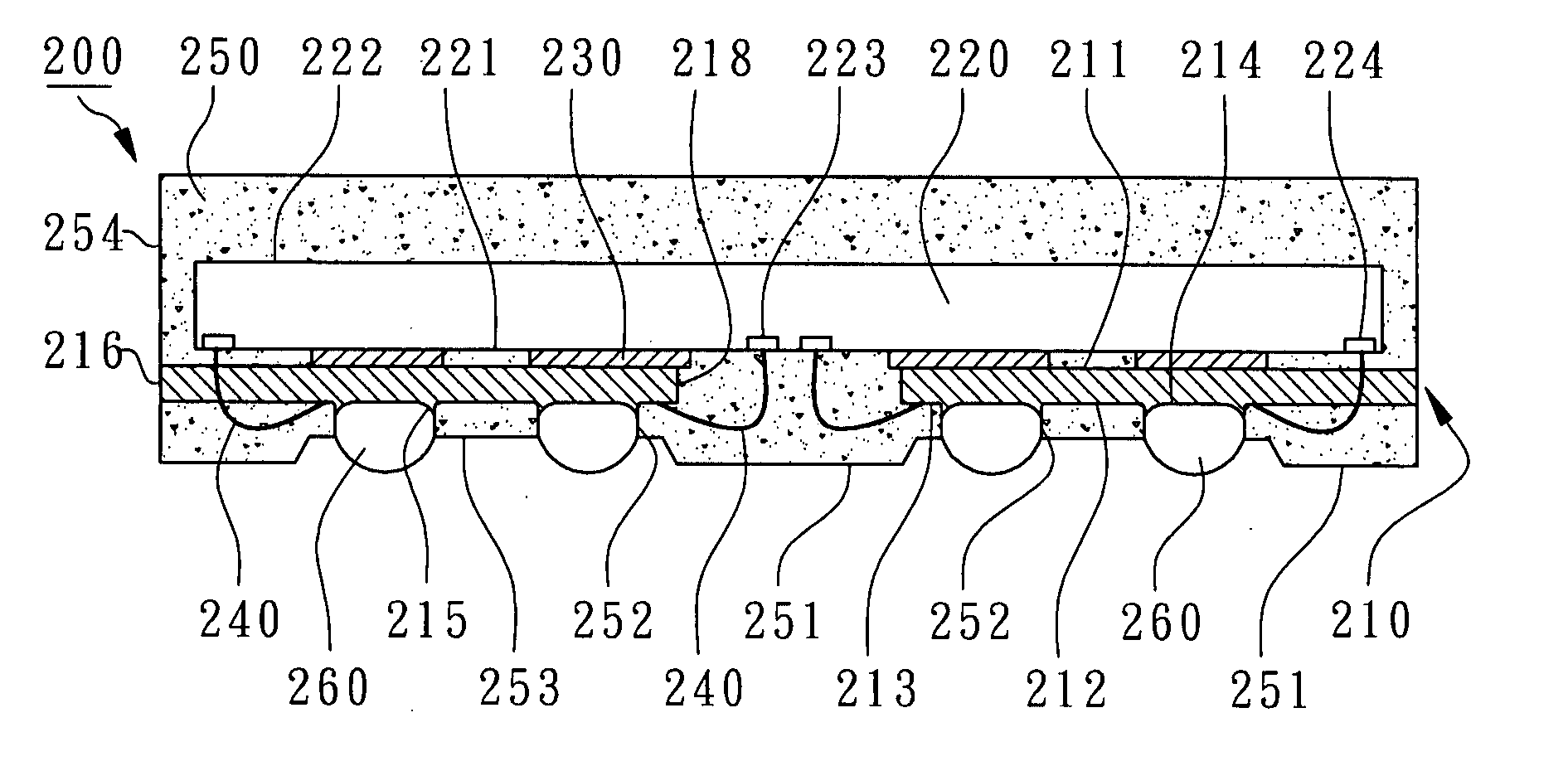
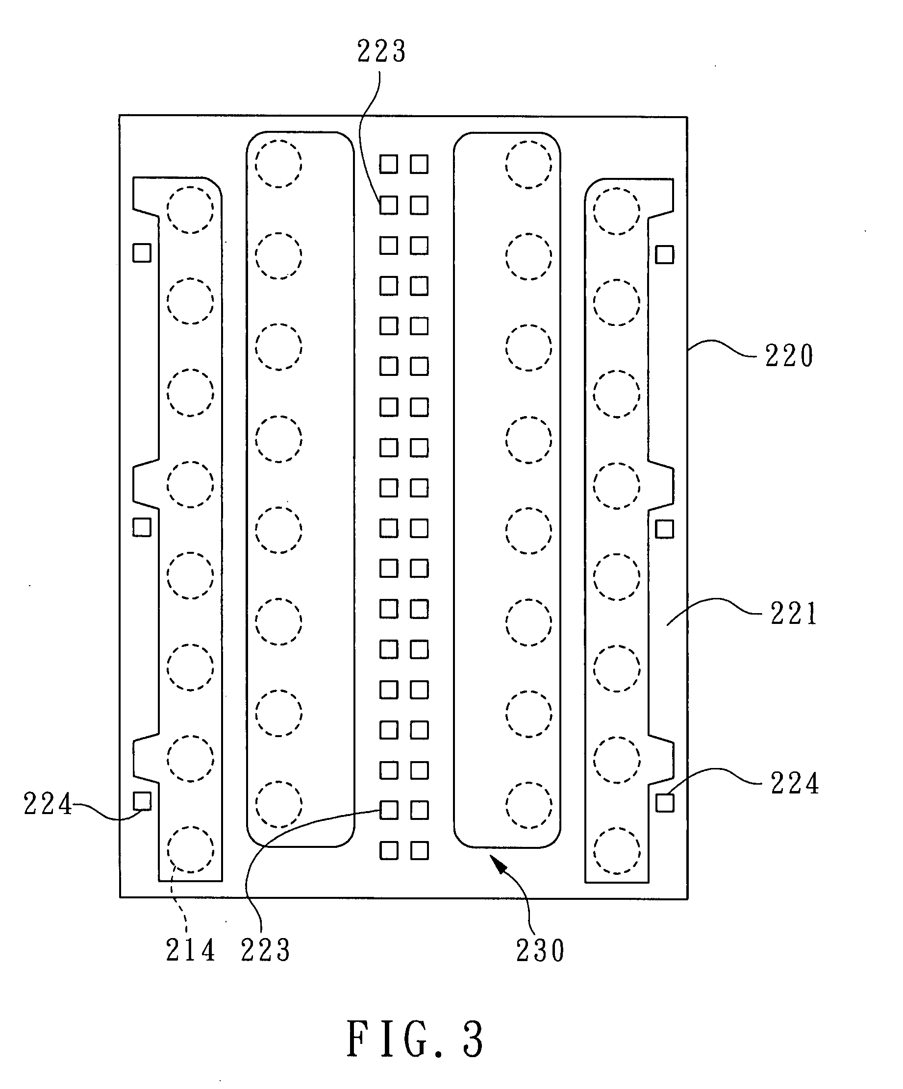
[0026]A BGA package with LOC configuration is disclosed according to the As shown in FIG. 2, a BGA package 200 primarily comprises a leadless leadframe having a plurality of leads 210, a chip 220, a die-attaching layer 230, a plurality of bonding wires 240, an encapsulant 250, and a plurality of solder balls 260. Normally, the materials of the leads 210 are metals such as copper, iron, or its alloys and are formed by punching or etching. Each lead 210 has a top surface 211 and a bottom surface 212 where the bottom surface 212 includes a wire-bonding area 213 and a ball-placement area 214. Each lead 210 further has an external end 216 between the top surface 211 and the bottom surface 212 away from the chip 220 and an internal end 218 extending toward a plurality of bonding pads 223 of the chip 220 where the external end 216 is exposed from one side of the encapsulant 250 in this embodiment. The wire-bonding areas 213 are located at the internal ends 218 of the corresponding leads 2...

third embodiment

[0046]Another BGA package 400 is revealed in the present invention, as shown in FIG. 8, primarily comprising a leadless leadframe having a plurality of leads 410, a first chip 420, a die-attaching layer 430, a plurality of first bonding wires 441, an encapsulant 450, and a plurality of solder balls 460. Each lead 410 has a top surface 411 and a bottom surface 412 where the bottom surface 412 includes a wire-bonding area 413 and a ball-placement area 414. The leads 410 have a plurality of lips 415 projecting from the bottom surfaces 412 to enclose the peripheries of the ball-placement areas 414. In the present embodiment, the leadless leadframe further has a plurality of bus leads 417 where the bus leads 417 are disposed adjacent to a plurality of internal ends 419 of the leads 410 and approximately perpendicular to the leads 410. The first chip 420 is disposed on the top surfaces 411 of the leads 410 and has an active surface 421 where a plurality of first bonding pads 423 and a plu...

fourth embodiment

[0049]As shown in FIG. 9, the present invention, another BGA package 500 primarily comprises a leadless leadframe having a plurality of leads 510, a chip 520, a die-attaching layer 530, a plurality of bonding wires 540, an encapsulant 550, and a plurality of solder balls 560. Each lead 510 has a top surface 511 and a bottom surface 512 where the bottom surface 512 includes a wire-bonding area 513 and a ball-placement area 514. Each lead 510 further has a lip 515 projecting from the bottom surface 512 and surrounding the peripheries of the ball-placement area 514. In the present embodiment, the lip 515 is a circular ring in a closed form to offer a non-planar ball pad. Each lead 510 further has an external end 516 formed between the top surface 511 and the bottom surface 512 away from the chip 520 where the external end 516 is encapsulated by the encapsulant 550 so that all of the leads 510 are encapsulated by the encapsulant 550 except the ball-placement areas 514. The leadframe fur...


PUM


Abstract

A BGA package primarily includes a leadless leadframe with a plurality of leads, a chip disposed on the leads, a die-attaching layer adhering to an active surface of the chip and the top surfaces of the leads, a plurality of bonding wires electrically connecting the chip to the leads, an encapsulant, and a plurality of solder balls. Each lead has a bottom surface including a wire-bonding area and a ball-placement area, moreover, a plurality of lips project from the bottom surfaces of the leads around the ball-placement areas. The encapsulant encapsulates the chip, the bonding wires, the die-attaching layer, and the top surfaces, the bottom surfaces except the ball-placement areas, and the laterals of the leads between the top surfaces and the bottom surfaces. A plurality of cavities are formed in the bottom of the encapsulant to expose the corresponding and embedded ball-placement areas. The lips have a plurality of internal sides exposed inside the cavities. The solder balls are disposed on the ball-placement areas and on the internal sides of the cavities to make the solder balls partially embedded in the corresponding cavities to offer non-planar ball pads. It is effective to resolve the solderability of the solder balls and to enhance the reliability of wire bonding and the stability of solder ball placement.

Description

CROSS REFERENCE TO RELATED APPLICATIONS[0001]This is a continuation-in-part of U.S. patent application Ser. No. 11 / 543,053, filed Aug. 21, 2007.FIELD OF THE INVENTION[0002]The present invention relates to semiconductor devices, and more particularly, to a Ball Grid Array (BGA) package with lead-on-chip (LOC) configuration.BACKGROUND OF THE INVENTION[0003]The conventional Ball Grid Array packages (BGA) are always using printed circuit boards as chip carriers. In one kind of BGA packages, the active surfaces of chips face to the printed circuit boards, and the bonding wires pass through the slots of the printed circuit boards. This kind of BGA package is often called Window BGA, Chip-On-Board BGA, or Chip-On-Substrate BGA.[0004]As shown in FIG. 1, a conventional BGA package 100 includes a printed circuit board 110, a chip 120, a die-attaching layer 130, a plurality of bonding wires 140, an encapsulant 150, and a plurality of solder balls 160. The printed circuit board 110 is made of B...

Claims


Application Information

Patent Timeline
Patent Type & Authority Applications(United States)
IPC IPC(8): H01L23/495H01L23/498
CPCH01L23/3114H01L2224/06136H01L23/49575H01L2224/48091H01L2224/4824H01L2224/48247H01L2224/4826H01L2224/83194H01L2224/83856H01L2924/01046H01L2924/01078H01L2924/01079H01L2924/1433H01L2924/15311H01L23/4951H01L2224/06135H01L2224/32145H01L2224/73215H01L2224/32245H01L2224/32225H01L24/48H01L2924/00014H01L2924/00H01L2224/451H01L24/45H01L2924/181H01L2224/05599H01L2924/00012
Inventor LIN, HUNG-TSUN
Owner CHIPMOS TECH INC
Why Eureka
Try Eureka