Organic Thin Film Transistors, Organic Light-emissive Devices and Organic Light-emissive Displays

Inactive Publication Date: 2010-08-12
CAMBRIDGE DISPLAY TECH LTD +1
View PDF8 Cites 12 Cited by
  • Summary
  • Abstract
  • Description
  • Claims
  • Application Information

AI Technical Summary

Benefits of technology

[0046]A spacer group may be provided between the attachment moiety and the dopant moiety. The spacer groups can be used to better dispose the dopant moieties within the OSC leading to better doping. Furthermore, the spacer groups can provide some flexibility in the surface onto which the OSC is to be deposited which can result in better film formation of the OSC thereon. The spacer group may be an alkylene chain, e.g. a C1-C20 alkylene chain. The spacer groups may be of different lengths so as to form a concentration gradient of dopant moiety which increases on approaching the source and drain electrodes.
[0047]For a bottom-gate device an organic dielectric material may be utilized to provide a large different

Problems solved by technology

For example, while the benzo-nitrile dopants disclosed in US 2005/133782 can be used as p-type dopants for certain OSC materials and can, apparently, provide some attachment properties to palladium, the benzo-nitril

Method used


Image

  • Organic Thin Film Transistors, Organic Light-emissive Devices and Organic Light-emissive Displays
  • Organic Thin Film Transistors, Organic Light-emissive Devices and Organic Light-emissive Displays
  • Organic Thin Film Transistors, Organic Light-emissive Devices and Organic Light-emissive Displays

Examples


Embodiment Construction

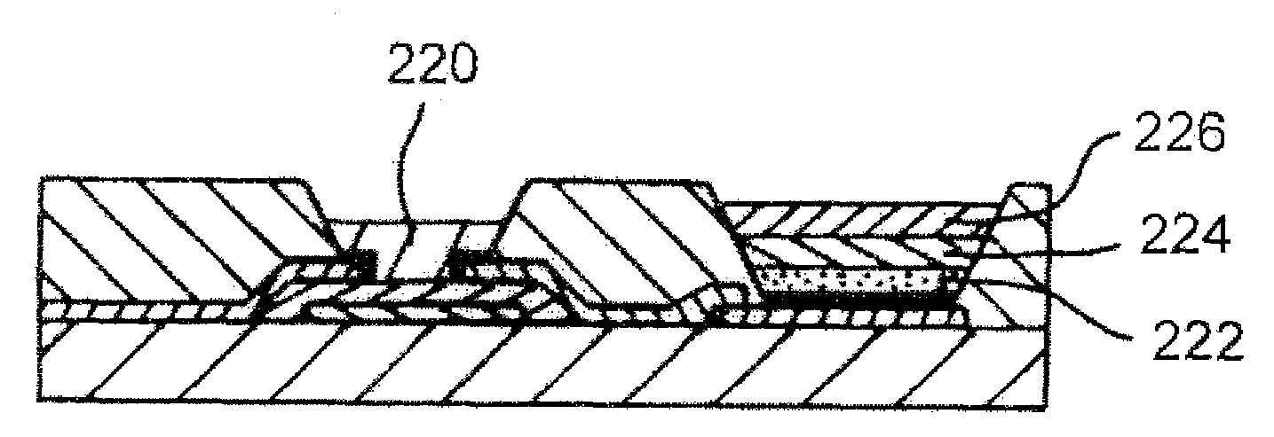
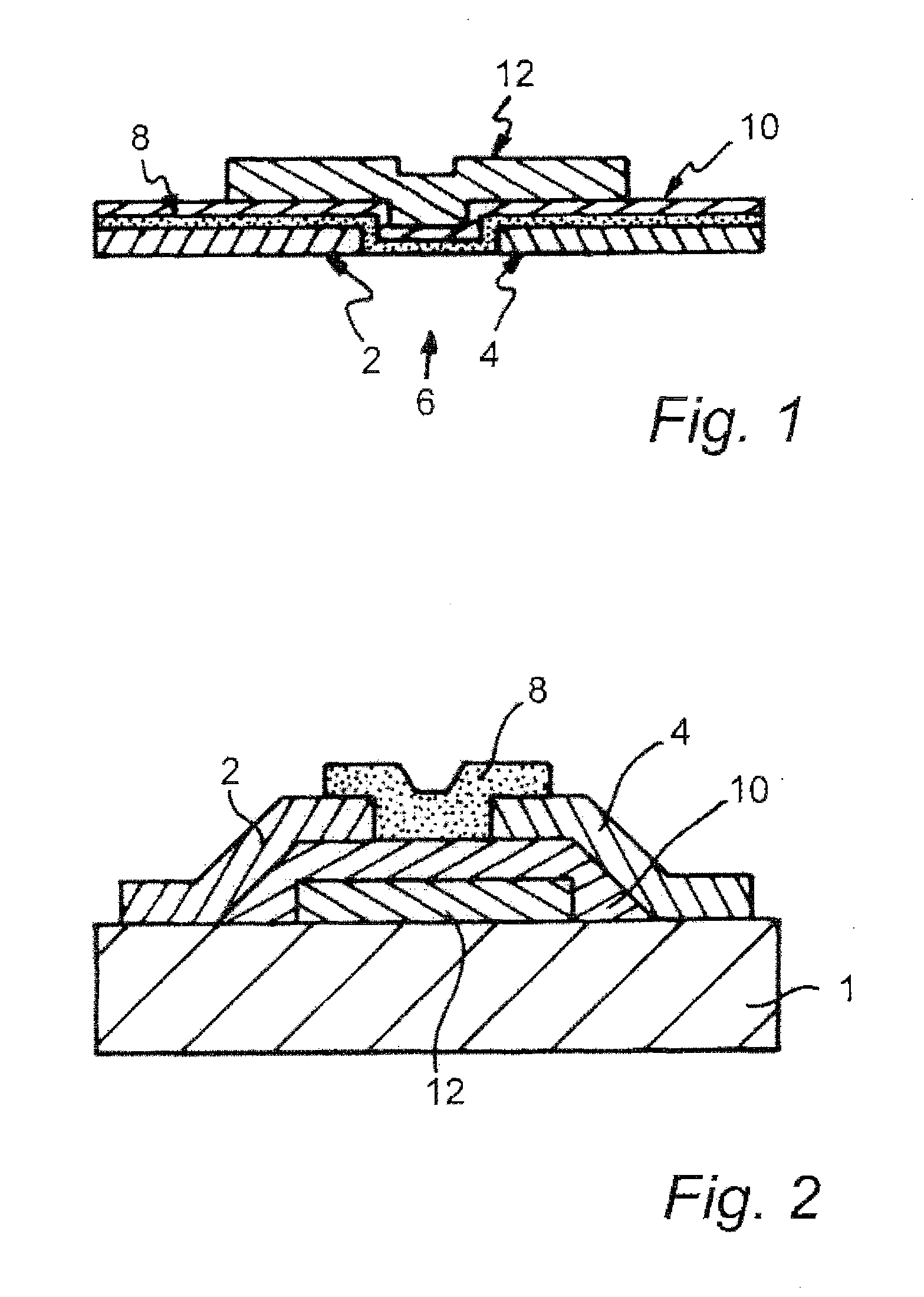
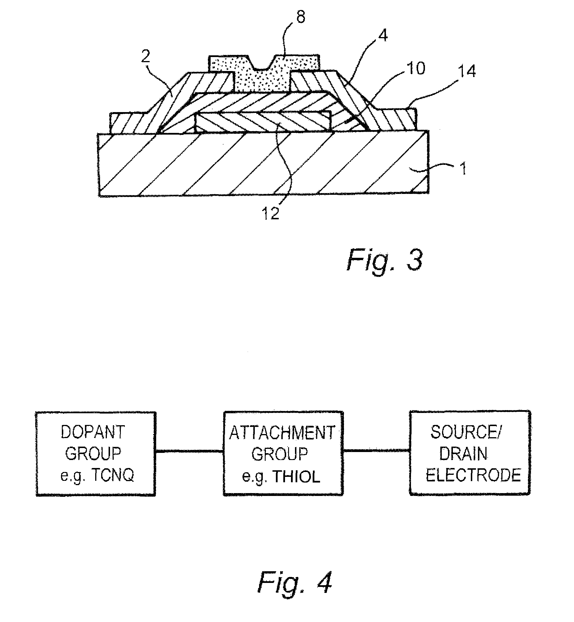
[0066]FIG. 3 shows a bottom-gate organic thin film transistor according to an embodiment of the present invention. The structure is similar to the prior art arrangement shown in FIG. 2 and for clarity like reference numerals have been used for like parts. The key difference of the arrangement shown in FIG. 3 is that the source and drain electrodes 2, 4 have disposed thereon a thin self-assembled layer of a material 14 comprising a dopant moiety for chemically doping the organic semi-conductive material by accepting or donating charge and a separate attachment moiety bonded to the dopant moiety and the source and drain electrodes.

[0067]A schematic diagram of the self-assembled layer 14 is illustrated in FIG. 4. For the example of gold or silver source-drain material, a dopant with a thiol attachment group could be used. A typical dopant molecule would include TCNQ, or F4TCNQ which has a deeper LUMO and is a more effective dopant (electron acceptor) with typical OSC materials.

[0068]Th...


PUM


Abstract

A method of manufacturing an organic thin film transistor, the method comprising: depositing a source and drain electrode; forming a thin self-assembled layer of material on the source and drain electrodes, the thin self-assembled layer of material comprising a dopant moiety for chemically doping an organic semi-conductive material by accepting or donating charge and a separate attachment moiety bonded to the dopant moiety and selectively bonded to the source and drain electrodes; and depositing a solution comprising a solvent and an organic semi-conductive material in a channel region between the source and drain electrode.

Description

FIELD OF INVENTION[0001]Aspects of the present invention relates to organic thin film transistors and methods of making the same. Further aspects of the present invention relate to organic light-emissive devices and methods of making the same. Yet further aspects of the present invention relate to organic light emissive displays comprising organic thin film transistors and organic light-emissive devices and methods of making the same.BACKGROUND OF THE INVENTION[0002]Transistors can be divided into two main types: bipolar junction transistors and field-effect transistors. Both types share a common structure comprising three electrodes with a semi-conductive material disposed therebetween in a channel region. The three electrodes of a bipolar junction transistor are known as the emitter, collector and base, whereas in a field-effect transistor the three electrodes are known as the source, drain and gate. Bipolar junction transistors may be described as current-operated devices as the ...

Claims


Application Information

Patent Timeline
IPC IPC(8): H01L51/56H01L51/40
CPCH01L51/0005H01L51/105H01L51/0545H10K71/135H10K10/84H10K10/466H10K59/12H10K10/462H10K50/80H10K71/00
Inventor HOTTA, SADAYOSHIHALLS, JONATHANWHITING, GREGORY
Owner CAMBRIDGE DISPLAY TECH LTD
Why Eureka
Try Eureka