Printed circuit board unit

a printed circuit board and unit technology, applied in the direction of printed circuit manufacturing, printed circuit aspects, final product manufacturing, etc., can solve the problems of complex assembling process, difficult to reduce the size of electronic devices, and the most occupied area of the pcb, so as to reduce the required amount of solder, reduce the size of the bubble, and improve the reliability and connection force of the welding structure

Inactive Publication Date: 2010-08-19
LITE ON ELECTRONICS (GUANGZHOU) LTD +1
View PDF8 Cites 7 Cited by
  • Summary
  • Abstract
  • Description
  • Claims
  • Application Information

AI Technical Summary

Benefits of technology

[0013]The present invention provides a printed circuit board unit and a reduced size of the bubbles inside the connecting pad in as SMT process. The

Problems solved by technology

It is not easy to reduce the size of electronic devices so that the devices occupy the most area of the PCB and the assembling processes are complex in the DIP method.
The large size of the bubble 2′ affects the reliability and the connection strength.
Furthermore, the large bubble 2′ results in the decreased conductivity and the efficiency of signal transmission.
Traditional solder

Method used


Image

  • Printed circuit board unit
  • Printed circuit board unit
  • Printed circuit board unit

Examples


first embodiment

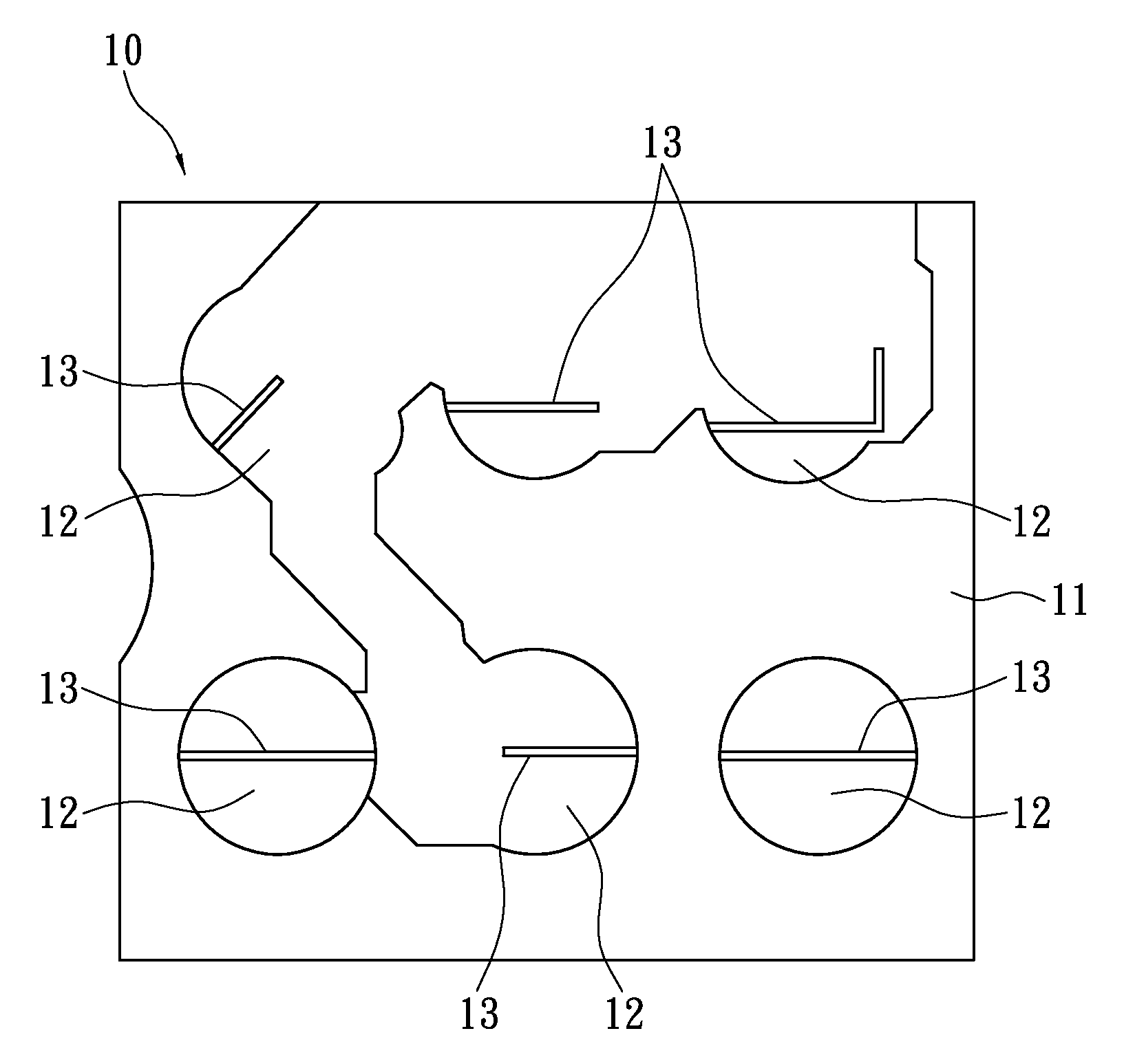
[0026]Please refer to FIG. 3, the first embodiment is shown. The connecting pad 12 has one venting opening 13 thereon. In the embodiment, the venting opening 13 is a through channel down to the substrate 11 so that the groove separates the connecting pad 12 into two sub pads 121, 122. The electronic device is weld on the two sub pads 121, 122. The method for manufacturing the venting opening 13 includes the following steps. In a layout step, there is a pattern of the venting opening 13 on the connecting pad 12. Simultaneously in the copper etching step for forming the connecting pad and circuit, the venting opening 13 is formed. Therefore, no extra process is applied in the present invention. After forming the venting opening 13 in the etching step, a step for coating a protection layer 15 adjacent to the connecting pad 12 is provided. In the present embodiment, a kind of paint is applied on the substrate 11 as the protection layer 15. The protection layer 15 has an insulating effec...

third embodiment

[0029]Please refer to FIG. 3, the present invention is shown. In the figure, the layout of the connecting pad 12 and the circuit is shown. In the present embodiment, the connecting pad 12 has two venting openings 13 thereon and the venting openings 13 can be through channel down to the substrate 11 or recess portion some distance into the connecting pad 12. The method for manufacturing the venting openings 13 is similar to the above embodiments.

[0030]Because of the separated two or more than two sub pads (i.e., the two sub pads 121, 122 in FIG. 3), the using area of the connecting pad 12 is decreased. Therefore, the required amount of welding material is reduced and the costs decrease. Moreover, the problem of electric shortcuts due to overflowing welding material is solved.

[0031]For improving the gas ventilation, there are two or more than two venting openings 13 formed on the connecting pad 12 when a lager electronic device is welded on the printed circuit board unit 10. Therefore...


PUM


Abstract

A printed circuit board unit includes a substrate and at least one connecting pad on the substrate. The connecting pad is used for electrically connecting to an electronic device by welding method. The connecting pad has at least one venting opening thereon. Therefore, the steam and gas by-produced in reflow soldering process can escape into the environment from the venting opening. Accordingly, the problem of large bubbles formed in the connecting pads is solved.

Description

BACKGROUND OF THE INVENTION[0001]1. Field of the Invention[0002]The present invention relates to a printed circuit board unit, in particular, to a printed circuit board unit with connecting pads having venting openings.[0003]2. Description of Related Art[0004]Electronic devices such as chips or components are assembled on a printed circuit board (PCB) by a dual in-line package (DIP) method or by surface mount technology (SMT). It is not easy to reduce the size of electronic devices so that the devices occupy the most area of the PCB and the assembling processes are complex in the DIP method. Therefore, SMT is widely used for assembling the components on PCBs today.[0005]The components are assembled on PCB 10′ by a welding method using solder or by reflow soldering using solder paints so as to connect electrically to the pad 12′ on PCB 10′, as shown in FIG. 1.[0006]PCB 10′ includes a substrate 11′, and circuit and pads 12′ arranged on the substrate 11′. PCB 10′ can be classified into...

Claims


Application Information

Patent Timeline
IPC IPC(8): H05K1/11
CPCH05K1/111H05K3/341H05K2203/1178H05K2201/0969H05K2201/09663Y02P70/50
Inventor CHANG, YUAN-CHILIN, WEN-LONGTSENG, KUO-LIANG
Owner LITE ON ELECTRONICS (GUANGZHOU) LTD
Why Eureka
Try Eureka