Modular solid-state millimeter wave (MMW) RF power source

a technology of solid-state millimeter wave and power source, which is applied in the direction of modular arrays, amplifiers with semiconductor devices/discharge tubes, and amplifiers with semiconductor devices. it can solve the problems of reducing the power output of each semiconductor device, requiring high voltage electrical power, and requiring high voltage, so as to reduce the number of radiating elements, reduce the number of chips, and simplify the operation. effect of circuit device functionality

Active Publication Date: 2010-08-19
RAYTHEON CO
View PDF14 Cites 11 Cited by
  • Summary
  • Abstract
  • Description
  • Claims
  • Application Information

AI Technical Summary

Benefits of technology

[0010]In an embodiment, the submodule includes an input antenna, a first power amplification stage and R output antennas. The first power amplification stage includes a 1:M1 power divider with an input coupled to the input antenna, M1 circuit devices, each including a solid-state amplifier chip, and M1 1:M2 power dividers with outputs coupled to the R output antennas. The submodule may include a second power amplification stage that includes M1*M2 circuit devices and M1*M2 1:M3 power dividers with outputs coupled to one of the R output antennas. The configuration of power dividers and circuit devices provides flexibility for selecting the number of amplifie

Problems solved by technology

However, such tubes are expensive, bulky, fragile, and require high voltage electrical power.
Thus MMW sources incorporating tubes are not readily portable.
Semiconductor devices

Method used


Image

  • Modular solid-state millimeter wave (MMW) RF power source
  • Modular solid-state millimeter wave (MMW) RF power source
  • Modular solid-state millimeter wave (MMW) RF power source

Examples


Embodiment Construction

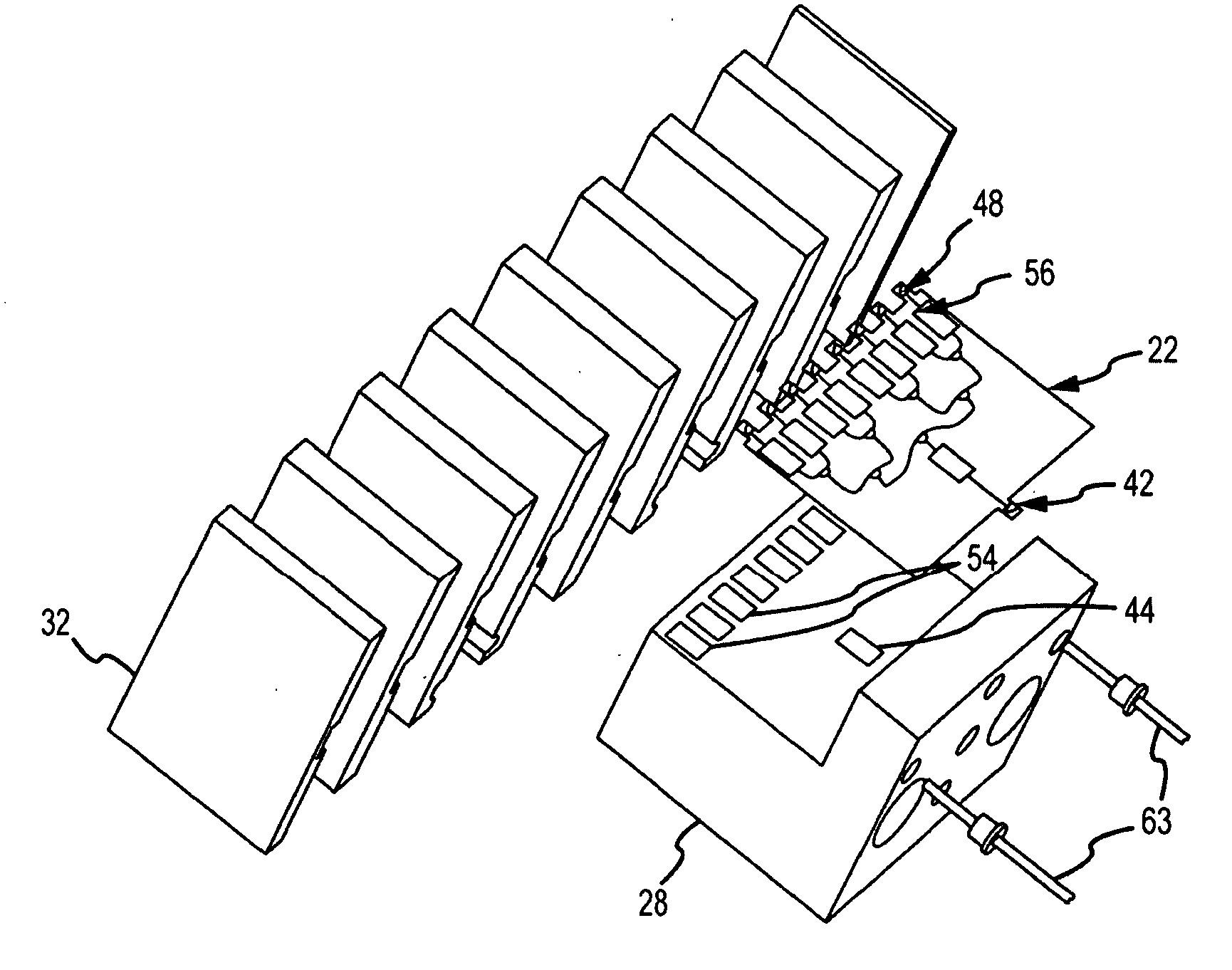
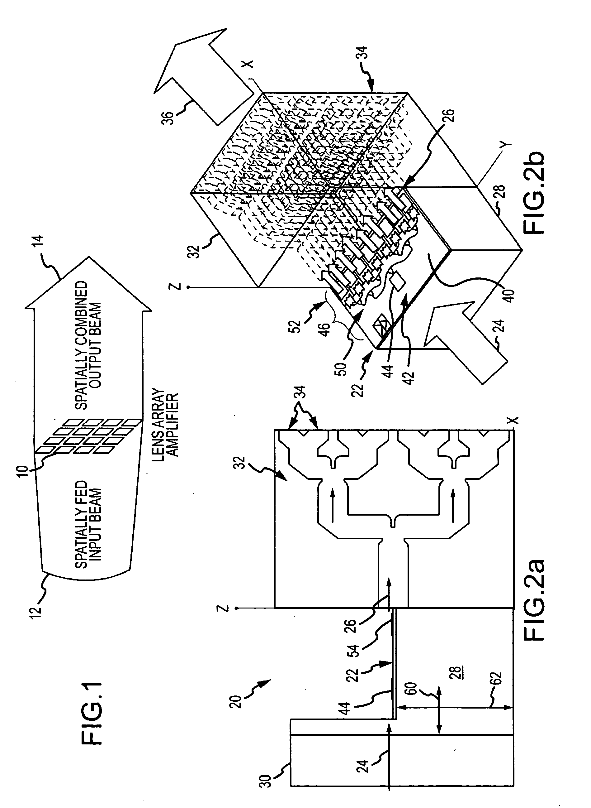
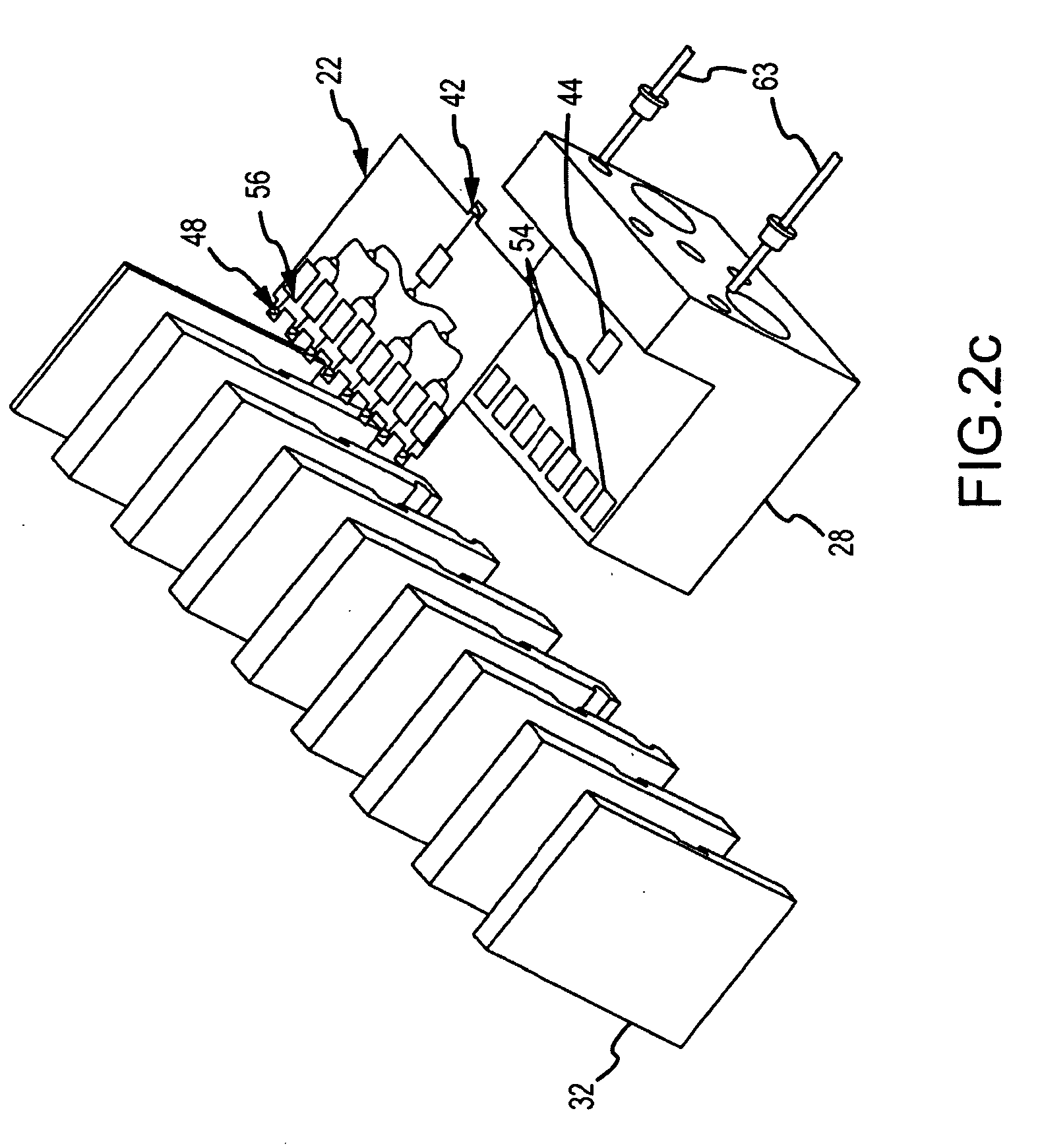
[0022]As shown in FIG. 1, the modular solid-state MMW power source of the present invention is a type of lens array amplifier. In general, a lens array amplifier 10 receives a spatially fed RF beam 12, divides the beam into channels and amplifies each channel using a solid-state amplifier chip to feed an array of radiating elements that spatially combine the amplified RF beams into a radiated RF beam 14. The array topology allows for the use of multiple amplifier chips, which together can provide the desired output power. Compared to the reflective topology, the lens array reduces chip material, hence reduces cost and the array of radiating elements can be more tightly spaced. Previous topologies of the lens array amplifier co-locate each amplifier chip with a radiating element. As a result, the number of amplifier chips is dictated by the size of the radiating array. Furthermore, the amplifier chips are packed in a dense array near the radiating face. These topologies are configure...


PUM


Abstract

A modular solid-state MMW power source based on a topology of the lens array amplifier provides both the flexibility to scale output power and effective thermal management. The modular power source includes a single submodule that uses one or more power dividers and one or more solid-state amplification stages to divide and amplify an RF input signal into R amplified RF signals. The submodule is mounted (suitably in the X-Y plane) on the surface of a heat sink, suitably coupled to a cold backplane, to remove heat. R 1:N low loss power dividers route the amplified RF signals to R*N radiating elements. Each of the 1:N power dividers suitably reside in the X-Z plane and are stacked in the Y direction to provide a planar output of the R*N radiating elements in the Y-Z plane. Placement of the amplifier chips on the single submodule decouples the number of amplifier chips, hence output power, from the number of radiating elements. Placement of the amplifier chips away from the radiating face provides a short path with large thermal cross-section through the heat sink to the backplane to remove heat. The topology can produce high output power combined with a high antenna gain to produce large power-aperture products previously only achievable with a Gyrotron. As amplifier chips become more powerful, the topology can be adapted to use fewer chips.

Description

RELATED APPLICATION INFORMATION[0001]This patent is related to copending application Ser. No. 12 / 237,312 entitled “Lens Array Module” filed Sep. 24, 2008 and copending application Ser. No. 11 / 841,580 entitled “Modular MMW Power Source” filed Aug. 20, 2007.BACKGROUND OF THE INVENTION[0002]1. Field of the Invention[0003]This invention relates to solid-state sources for millimeter wave (MMW) RF power, and to high power sources for W-band applications in particular.[0004]2. Description of the Related Art[0005]Sources of medium and high power, MMW radiation can be applied in communications systems and in directed energy weapons. While lower frequency MMW wave applications can now be satisfied with solid-state sources, high power sources for the W-band (75 GHz to 110 GHz) traditionally incorporate tubes such as magnetrons or Gyrotrons. Gyrotrons are effective because the large output power is combined with a very high gain antenna to produce a large power-aperture. However, such tubes are...

Claims


Application Information

Patent Timeline
IPC IPC(8): H04B1/40
CPCH01P5/12H01Q3/46H01Q21/0025H03F2200/321H01Q21/064H03F3/602H01Q21/0075
Inventor LOWELL, REID F.BROWN, KENNETH W.GRITTERS, DARIN M.BROWN, ANDREW K.SOTELO, MICHAEL J.DOLASH, WILLIAM E.FEENSTRA, TRAVIS B.
Owner RAYTHEON CO
Why Eureka
Try Eureka