High-frequency sputtering device

a sputtering device and high-frequency technology, applied in the direction of electrolysis components, vacuum evaporation coatings, coatings, etc., can solve the problems of high-energy positive ions damage a film during formation, the rate of magnetoresistance change is also reduced, etc., to achieve low junction resistance and high rate of magnetoresistance change

Active Publication Date: 2010-08-26
CANON ANELVA CORP
View PDF103 Cites 30 Cited by
  • Summary
  • Abstract
  • Description
  • Claims
  • Application Information

AI Technical Summary

Benefits of technology

[0011]However, a very thin film is demanded for a recent semiconductor device. Especially, since the thickness of crystalline insulating film MgO used for a tunnel barrier layer of a magnetoresistive thin film is very thin, the insulating film has to be grown in a highly oriented manner from an initial stage of its growth. For this reason it is important to intentionally control a substrate bias potential that changes as an insulating film is gradually deposited on the substrate, so that the bias potential is suppressed within such a potential range that promotes surface diffusion of sputtering atoms on the substrate surface and does not damage the film. The object of the present invention is to produce a magnetoresistive thin film in which low junction resistance is attained while a high rate of magnetoresistance change is maintained by adjusting the substrate potential so that self bias with respect to a substrate is controlled to give good crystalline orientation from an initial stage of growth of an insulating film.
[0013]According to the high-frequency sputtering device which controls the magnitude of self-bias applied on a substrate by the variable impedance mechanism of the present invention, a magnetoresistive thin film having low junction resistance while maintaining a high rate of magnetoresistance change, can be produced.

Problems solved by technology

Although, it is possible to reduce junction resistance by reducing the thickness of the tunnel barrier layer of MgO film, there has been a problem that the rate of magnetoresistance change is also reduced at the same time.
However, if a bias potential on the substrate is too high, a problem that high energy positive ions damage a film during formation, will occur.

Method used


Image

  • High-frequency sputtering device
  • High-frequency sputtering device
  • High-frequency sputtering device

Examples


first embodiment

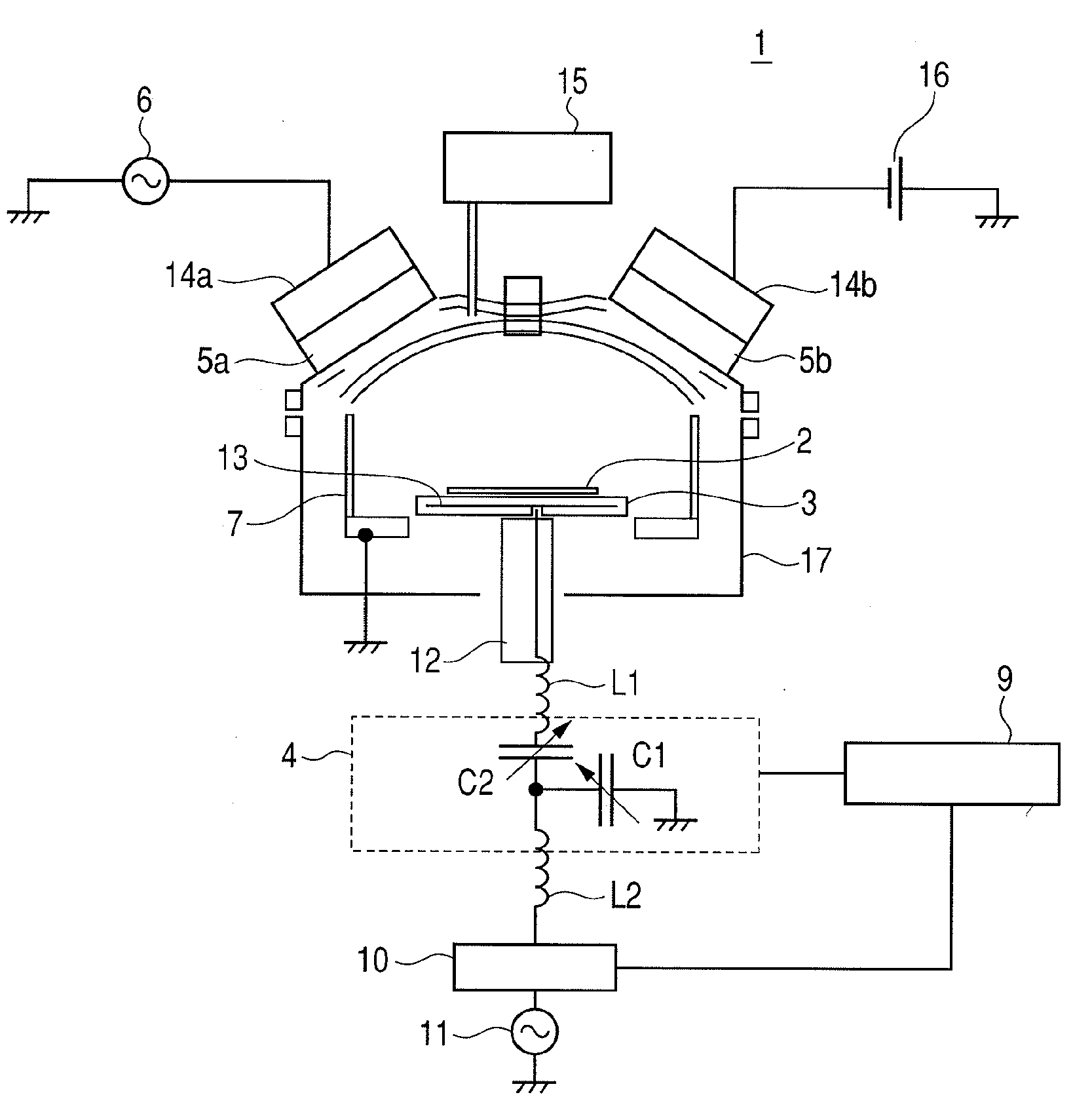
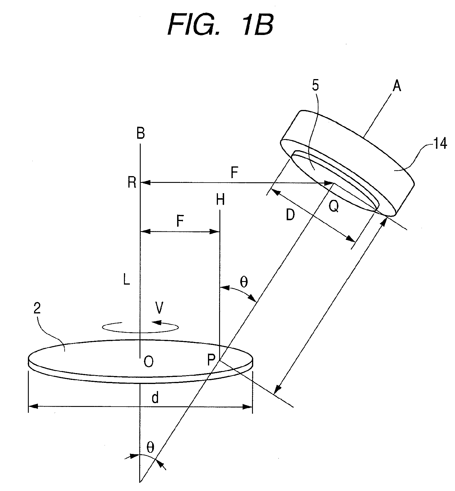
[0031]FIG. 1A is a schematic view of a high-frequency sputtering device 1 exhibiting the feature of the present invention. With reference to FIG. 1A, the configuration of the high-frequency sputtering device 1 to which the present invention can be applied, will be described. The sputtering device 1 includes sputtering cathodes 14a and 14b, each provided with a target mounting table. A target 5a and a target 5b are mounted on the target mounting tables of the cathode 14a and the cathode 14b, respectively. In the present embodiment, the target 5a is an insulator MgO target and the target 5b is a metal Ta target, and however the targets can be suitably altered by a user. The cathode 14a is connected to a grounded high-frequency power supply 6 via a blocking capacitor (not illustrated in the figure). Here, the high-frequency power supply 6 is referred to as such a power supply that can supply power of 200 to 1000 W. The other cathode 14b is connected to a grounded DC power supply 16. Th...

second embodiment

[0044]With reference to FIG. 2, the configuration of a high-frequency sputtering device according to the second embodiment will be described. As illustrated in FIG. 2, an electrode 13 is disposed inside a substrate holder 3 on which a substrate 2 is mounted. On the electrode 13, an inflow-electron detection sensor (Vdc detection sensor) 18 for detecting the value of current by taking in electrons flown from plasma is disposed. The inflow-electron detection sensor 18 is constituted by a hole formed so that the electrode 13 disposed inside the substrate holder 3 is exposed, and detects electrons by inflow of the electrons in plasma into the electrode 13 through the hole.

[0045]Here, Vdc is difference in a potential between those of a ground and a substrate, i.e., the self-bias applied to the substrate. The high-frequency sputtering device of the present embodiment is provided with an arithmetic circuit 8 including arithmetic section 8a for converting the current value detected by the i...

third embodiment

[0050]Now, with reference to FIG. 4, the configuration of a high-frequency sputtering device according to the third embodiment will be described. In the present embodiment also, a substrate 2 is placed on a substrate holder 3, and a variable impedance mechanism 4 including capacitors C1 and C2 and coils L1 and L2 is electrically connected to an electrode 13 disposed inside the substrate holder 3. The variable impedance mechanism 4 is grounded. Note that, in FIG. 3, although a vacuum chamber 17, cathodes 14a and 14b, a high-frequency power supply 6, a DC power supply 16, a metal shield 7, targets 5a and 5b, and a gas supply device 15 etc. are not illustrated, they are disposed therein like the high-frequency sputtering device 1 illustrated in FIG. 1. In addition, although only the capacitors C1 and C2 and the coils L1 and L2 are illustrated in FIG. 4, selection of capacitors C and coils L and their combination can be changed appropriately in design according to an embodiment. Even if...


PUM

PropertyMeasurementUnit
poweraaaaaaaaaa
pressureaaaaaaaaaa
pressureaaaaaaaaaa

Abstract

Provided is a high-quality magnetoresistive thin film by using a method of controlling self bias of a high-frequency sputtering device. In order to control the self bias for the substrate by adjusting a substrate potential, the high-frequency sputtering device according to the present invention includes: a chamber; evacuation means for evacuating the inside of the chamber; gas introduction means for supplying a gas into the chamber; a substrate holder provided with a substrate mounting table; rotation drive means capable of rotating the substrate holder; a sputtering cathode provided with a target mounting table and arranged such that the surface of the target mounting table is non-parallel to the surface of the substrate mounting table; an electrode disposed inside the substrate holder; and a variable impedance mechanism electrically connected to the electrode, for adjusting the substrate potential on the substrate holder.

Description

CROSS-REFERENCES TO RELATED APPLICATIONS[0001]This application is a continuation application of International Application No. PCT / JP2008 / 065485, filed on Aug. 29, 2008, the entire contents of which are incorporated by reference herein.[0002]This application also claims the benefit of priorities from PCT International Application No. PCT / JP2007 / 069459 filed on Oct. 4, 2007 and Japanese Patent Application No. 2008-215386 filed on Aug. 25, 2008, the entire contents of which are incorporated herein by reference.BACKGROUND OF THE INVENTION[0003]1. Field of the Invention[0004]The present invention relates to a high-frequency sputtering device for manufacturing a magnetic reproducing head of a magnetic disc driver, a storage element of a magnetic random access memory and a magnetic sensor, and a manufacturing method thereof.[0005]2. Related Background Art[0006]Since a tunnel magnetoresistive thin film using insulating film MgO as a tunnel barrier layer exhibits extremely high rate of magne...

Claims


Application Information

Patent Timeline
Patent Type & Authority Applications(United States)
IPC IPC(8): C23C14/34
CPCC23C14/081C23C14/225C23C14/345C23C14/3464H01L43/12H01J37/3444C23C14/352C23C14/50H01J37/3417H01J37/3438C23C16/4586H10N50/01
Inventor NAGAMINE, YOSHINORINAKAMURA, KANTOTSUNEKAWA, KOJI
Owner CANON ANELVA CORP
Why Eureka
Try Eureka