Semiconductor memory device and method of manufacturing the same

a memory device and semiconductor technology, applied in the field of semiconductor memory devices, can solve the problems of increasing production costs, complex formation of capacitors with effective capacitance in a small area, etc., and achieve the effect of improving the high density integration of semiconductor memory devices

Active Publication Date: 2010-08-26
SAMSUNG ELECTRONICS CO LTD
View PDF4 Cites 7 Cited by
  • Summary
  • Abstract
  • Description
  • Claims
  • Application Information

AI Technical Summary

Benefits of technology

[0006]It is therefore a feature of an embodiment to provide a semiconductor memory device with a vertical active pillar surrounded by vertically arranged gate electrodes on sidewalls of the active pillar in order to improve high density integration of the semiconductor memory device.

Problems solved by technology

However, miniaturization of the field effect transistor may cause a short channel effect in the DRAM device, and the process technology for forming the capacitor with an effective capacitance in a small area may be complex and increase production costs.

Method used


Image

  • Semiconductor memory device and method of manufacturing the same
  • Semiconductor memory device and method of manufacturing the same
  • Semiconductor memory device and method of manufacturing the same

Examples


first embodiment

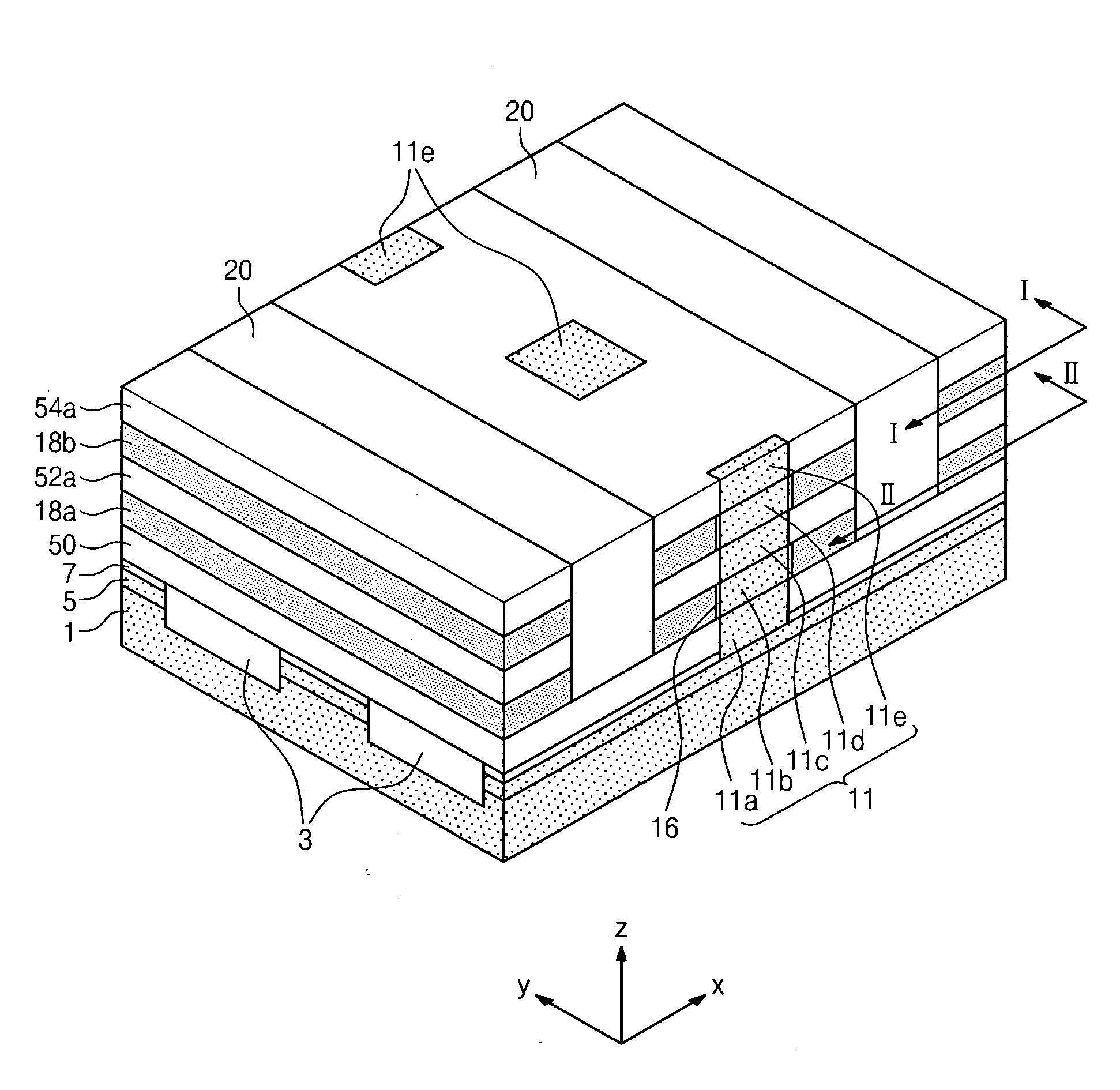
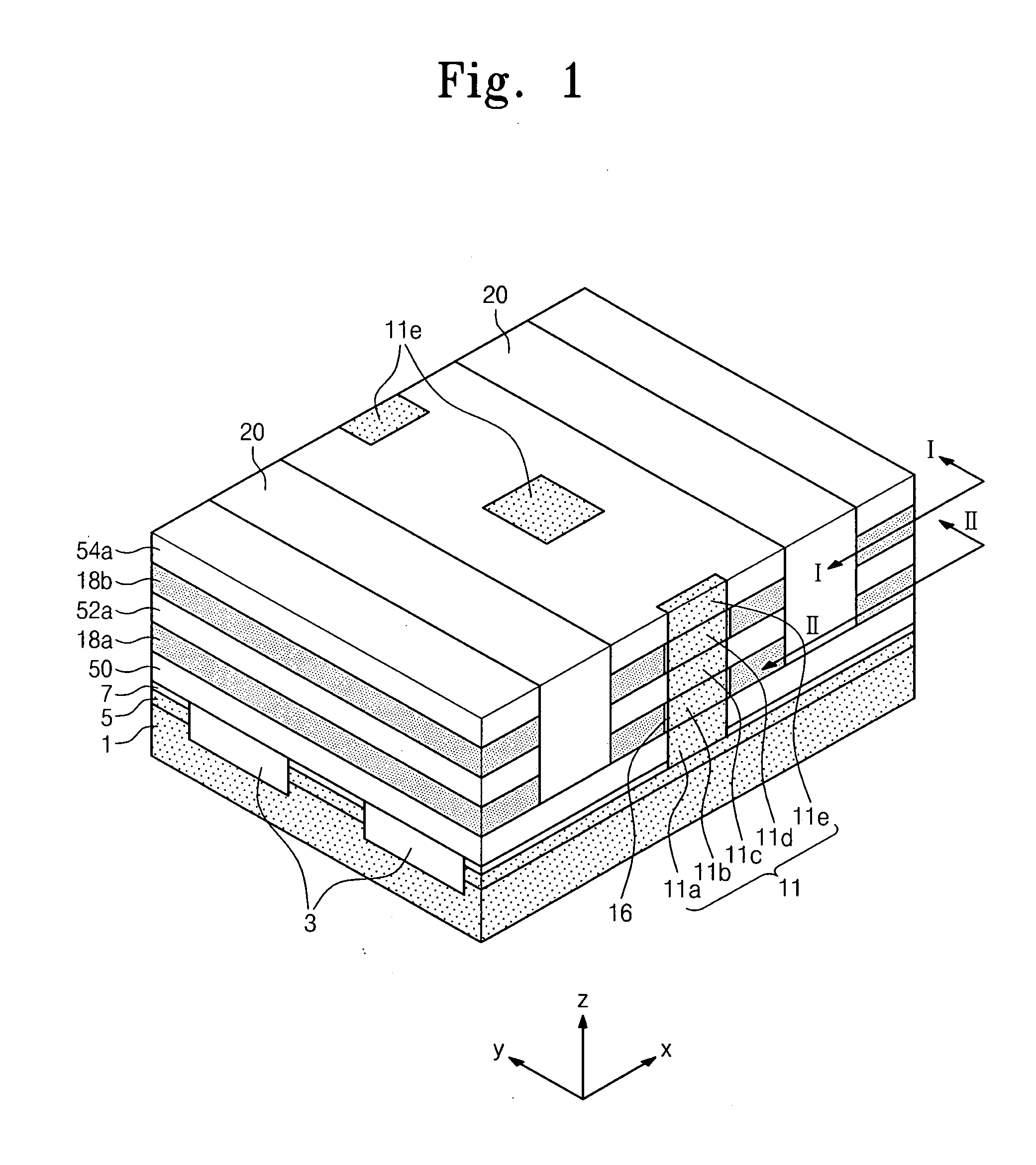
[0035]FIG. 1 illustrates a perspective view of a semiconductor memory device in accordance with an example embodiment. FIG. 2 illustrates a top plan view along line I-I or II-II of FIG. 1.

[0036]Referring to FIGS. 1 and 2, in a semiconductor memory device in accordance with an embodiment, a semiconductor substrate 1 may have a top plan in first and second directions x and y, e.g., the first and a second directions x and y may be orthogonal to each other. That is, a top surface of the semiconductor substrate 1 may be positioned in the xy-plane, as illustrated in FIG. 1. A plurality of device isolation layers 3 may extend in the first direction x in the semiconductor substrate 1. An impurity-doped region 5 may be formed in the semiconductor substrate 1 adjacent to the device isolation layer 3, e.g., between two adjacent device isolation layers 3. An active pillar 11 may protrude from a predetermined region of the semiconductor substrate 1, e.g., the active pillar 11 may be on the impur...

second embodiment

[0061]FIG. 15 illustrates a perspective view of a semiconductor memory device in accordance with another embodiment. FIG. 16 illustrates a top plan view along line I-I or II-II of FIG. 15. The second embodiment may be substantially the same as the first embodiment described previously with reference to FIGS. 1-14, with the exception of having the gate electrodes surround three surfaces of the active pillar, as opposed to four surfaces.

[0062]In detail, referring to FIGS. 15 and 16, the first and second body regions 11b and 11d may include four successive side surfaces, e.g., defining a pillar with a square cross-section as viewed from top view, and first and second gate electrodes 28a and 28b surrounding three of the four side surfaces. In other words, the first and second gate electrodes 28a and 28b may have a comb shape running in the second direction y, i.e., a linear structure along the y direction with protrusions along the x direction that are spaced apart along the y direction...

third embodiment

[0069]FIG. 20 illustrates a perspective view of a semiconductor memory device in accordance with another embodiment. FIG. 21 illustrates a top plan view along line I-I or II-II of FIG. 20. The third embodiment may be substantially the same as the first embodiment described previously with reference to FIGS. 1-14, with the exception of having the gate electrodes extend only along one surface of the active pillar with the gate insulating layers therebetween.

[0070]Referring to FIGS. 20 and 21, in a semiconductor memory device in accordance with the present embodiment, first and second gate electrodes 38a and 38b may be in contact with, e.g., only, one side surface of the active pillar 11, e.g., via the gate insulating layer 16. For example, each of the first and second gate electrodes 38a and 38b may have a line shape running in the second direction y. An insulating pattern 80 may be disposed between active pillars 11, i.e., between adjacent active pillars arranged along the second dir...


PUM


Abstract

A semiconductor memory device includes a plurality of active pillars protruding from a semiconductor substrate, a first gate electrode disposed on at least one sidewall of the active pillar, a first gate insulating layer being disposed between the active pillar and the first gate electrode, a second gate electrode disposed on at least one sidewall of the active pillar over the first gate electrode, a second gate insulating layer being disposed between the active pillar and the second gate electrode, first and second body regions in the active pillar adjacent to respective first and second respective electrodes, and first through third source / drain regions in the active pillar arranged alternately with the first and second body regions.

Description

BACKGROUND[0001]1. Field[0002]The present disclosure relates to semiconductor memory devices and methods of manufacturing the same.[0003]2. Description of the Related Art[0004]Generally, a dynamic random access memory (DRAM) device may include a field effect transistor controlling a read / write operation and a capacitor storing a charge. A high integration of a DRAM device has been continuously improved by miniaturization of the field effect transistor and a process technology, e.g., a technology for forming a stack capacitor or a deep trench capacitor, for obtaining an effective capacitance of the capacitor in a small area. However, miniaturization of the field effect transistor may cause a short channel effect in the DRAM device, and the process technology for forming the capacitor with an effective capacitance in a small area may be complex and increase production costs.SUMMARY[0005]Embodiments are therefore directed to a semiconductor memory device and a method of manufacturing t...

Claims


Application Information

Patent Timeline
Patent Type & Authority Applications(United States)
IPC IPC(8): H01L27/108
CPCH01L27/0688H01L27/105H01L27/10844H01L27/10802H01L27/108H10B12/20H10B12/01H10B12/00A41B9/001A41B9/04A41D1/002A41D13/1281G06F21/32G08B21/02
Inventor JEON, SANGHUNLEE, JONGWOOKKANG, JONG-HYUKPARK, HEUNGKYU
Owner SAMSUNG ELECTRONICS CO LTD
Why Eureka
Try Eureka