Semiconductor switching device

a switching device and semiconductor technology, applied in electronic switching, pulse technique, instruments, etc., can solve the problems of ensuring safe shut off, shutting off switching elements, and serious problems such as arm short circuits, and achieve the effect of suppressing the damage to switching elements due to arm short circuits and large curren

Inactive Publication Date: 2010-08-26
MITSUBISHI ELECTRIC CORP
View PDF7 Cites 16 Cited by
  • Summary
  • Abstract
  • Description
  • Claims
  • Application Information

AI Technical Summary

Benefits of technology

[0011]In view of the above-described problems, objects of the present invention is to provide a semiconductor switching device in which the damage to the switching elements due to the arm short circuit is suppressed, the switching loss due to the recovery current of the diode is suppressed, and capable of handling a large current.

Problems solved by technology

There may arise a problem wherein the DC source is short circuited by the two switching elements (this short circuit of the DC source is called as an arm short circuit, hereinafter), since the two switching elements are switched into an ON state simultaneously due to such as a malfunction.
The arm short circuit is a serious problem because it damages the switching element.
There arises a problem of the difficulty in ensuring the safe shut off of the switching elements since shutting off the switching elements in a very short period of time is difficult.
Moreover, detecting the arm short circuit in a short period of time and shutting off the switching elements quickly may be difficult depending on the circuit configuration.
However, when the switching elements switched to on state again, there arises a problem of a switching loss caused by the recovery current that is generated in the diode.
When the semiconductor elements are connected in parallel with each other, there arises a problem of increase of the inductance between the chips.
Accordingly, a back electromotive force voltage, which is the product of the inductance and the di / dt, is increased when a lot of switching elements are connected in parallel, thereby causing a problem of lowering the switching speed.
However, when the switching elements and the diodes are mounted closely adjacent each other, there arises a problem of the obstruction of radiation of heat, for example, from the semiconductor elements.

Method used


Image

  • Semiconductor switching device
  • Semiconductor switching device
  • Semiconductor switching device

Examples


first embodiment

[0027]The first embodiment of the present invention will now be described with reference to FIGS. 1 to 3. Like materials and elements are designated by the same reference numerals and may not be redundantly described. This is also true for the other embodiments of the present invention.

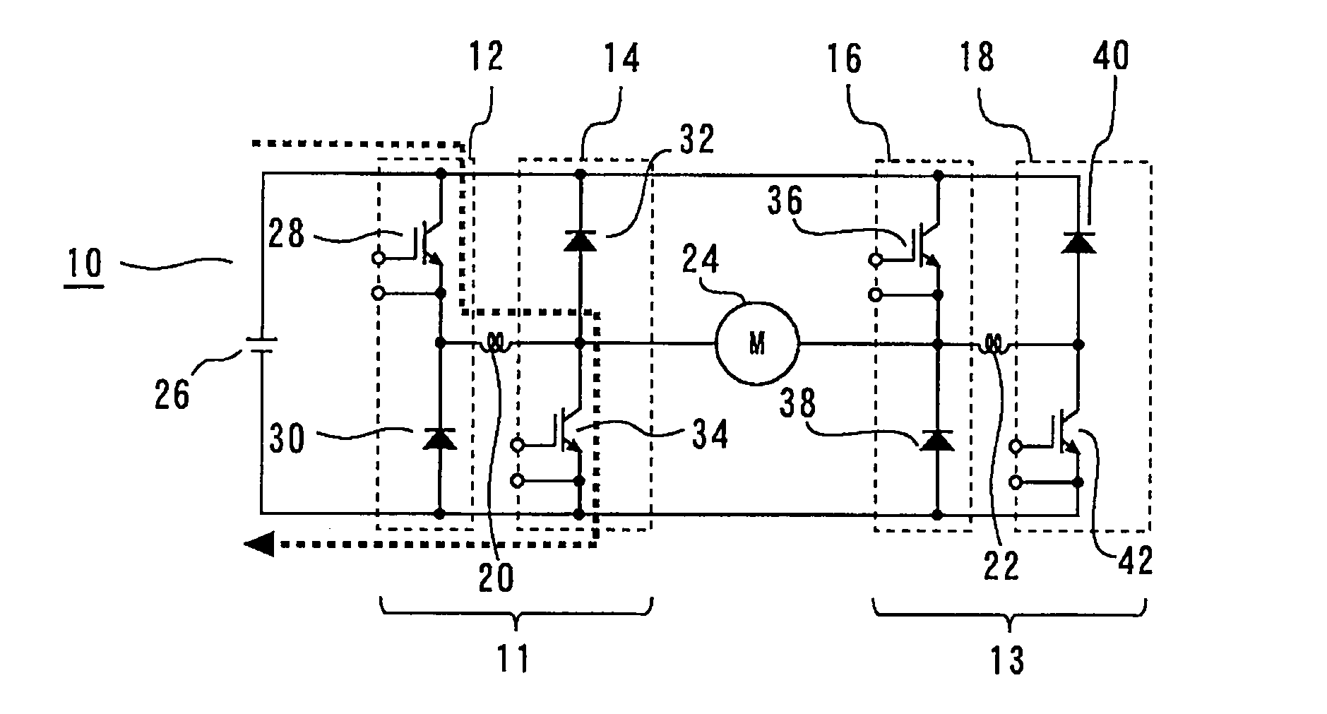
[0028]FIG. 1 is a circuit diagram of a semiconductor switching device according to the first embodiment. A first power control part 11 and a second power control part 13 are provided with the semiconductor switching device 10. The first power control part 11 and the second power control part 13 are a half bridge circuit, respectively. Further, the first power control part 11 and the second power control part 13 are connected to a load 24 that is subject to control. The load 24 of the present embodiment may be made of, but is not limited to, a motor. The load 24 is connected to a DC source 26 via the semiconductor switching device 10 that consists of the first power control part 11 and the second power...

second embodiment

[0062]The second embodiment will now be described with reference to FIGS. 6 and 7. FIG. 6 is explained firstly. Although a Semiconductor switching device shown in FIG. 6 is almost identical to the semiconductor switching device shown in FIG. 1, there is a difference in a semiconductor element. Namely, a first switching element 208, a second switching element 212, a third switching element 216 and a fourth switching element 220 are composed of a power MOSFET, respectively in this embodiment. Here, parasitic diodes 210, 214, 218 and 222 connected parallelly and inversely to each of the switching elements are shown only for the purpose of explaining the reverse conduction of the power MOSFET. Therefore, the parasitic diodes are not independently arranged actually.

[0063]Here, the operation of the semiconductor switching device will be described. First of all, the first switching element 208 and the fourth switching element 220 are set in the ON state so as to execute the PWM control of ...

third embodiment

[0067]The third embodiment will now be described with reference to FIGS. 8 and 9. FIG. 8 is explained firstly.

[0068]Although a semiconductor switching device shown in FIG. 8 is almost identical to the semiconductor switching device shown in FIG. 1, they differs in that diodes 608, 610, 612 and 614 connected parallelly and inversely to each of the switching elements are provided to FIG. 8. Here, a reverse recovery charge in diode 608 connected parallelly and inversely to the first switching element 28 is lower than a reverse recovery charge in the second diode 32. This relationship is also true for the reverse recovery charge in diode 610 and the first diode 30, the diode 612 and the fourth diode 40 as well as the diode 614 and the third diode 38.

[0069]Here, a backward voltage might be momentarily applied to the switching element because of the floating impedance of the circuit wiring. However, in this embodiment, the above mentioned backward voltage, that might be momentarily applie...


PUM


Abstract

A semiconductor switching device includes a power control part, which includes a voltage dropping chopper circuit having a first switching element and a first diode, a voltage boosting chopper circuit having a second switching element and a second diode, and an inductance. And the inductance is connected such that an unusual current caused by the arm short circuit is forced to pass through the inductance.

Description

BACKGROUND OF THE INVENTION[0001]1. Field of the Invention[0002]The present invention relates to a semiconductor switching device for controlling voltage to be applied to a load.[0003]2. Background Art[0004]A semiconductor switching device has been used, such as an inverter for controlling a rotating speed of a motor, or a half bridge circuit which is provided for an inverter bridge circuit used as, for example, an AC source. A power element such as a power MOSFET or an IGBT (Insulated Bipolar Gate Transistor) is used as a semiconductor element since the semiconductor element used in the semiconductor switching device needs to handle a large current.[0005]A load is subject to being controlled by the semiconductor switching device and is connected to an AC source via the semiconductor switching device. The switching element, which is provided to the semiconductor switching device, performs a switching operation according to a driving signal produced by a control circuit such that des...

Claims


Application Information

Patent Timeline
Patent Type & Authority Applications(United States)
IPC IPC(8): G05F1/618G05F1/613
CPCH03K17/08142H03K17/6871H03K17/163H03K17/08148H01L2224/48091H01L2224/48227H01L2224/49111H01L2224/49175H01L2224/0603H01L2924/13055H01L2924/13091H01L2924/00014H01L2924/00
Inventor KORA, MASAYUKITABATA, MITSUHARU
Owner MITSUBISHI ELECTRIC CORP
Why Eureka
Try Eureka