Low cost soi substrates for monolithic solar cells

a solar cell and low-cost technology, applied in the field of semiconductoron-insulator (soi) substrates, can solve the problems of soi substrate cost, soi material cost, and both relatively high cost, and achieve the effect of reducing the defect density

Inactive Publication Date: 2010-09-02
GLOBALFOUNDRIES INC
View PDF8 Cites 165 Cited by
  • Summary
  • Abstract
  • Description
  • Claims
  • Application Information

AI Technical Summary

Benefits of technology

[0016]In another embodiment of the present invention, the stack of amorphous Si-containing layers includes a non-highly p-type doped amorphous Si-containing layer having a dopant concentration less than the first p-type doped amorphous Si-containing layer interposed between the semiconductor region of the underlying substrate and the first p-type doped amorphous Si-containing layer. In yet a further embodiment of the present invention, a highly p-type doped amorphous Si-containing layer is formed onto a major surface of the second p-type doped amorphous Si-cont

Problems solved by technology

One fundamental problem associated with the monolithic integration of solar cells is the cost of the SOI substrate.
Both of these k

Method used


Image

  • Low cost soi substrates for monolithic solar cells
  • Low cost soi substrates for monolithic solar cells
  • Low cost soi substrates for monolithic solar cells

Examples


Embodiment Construction

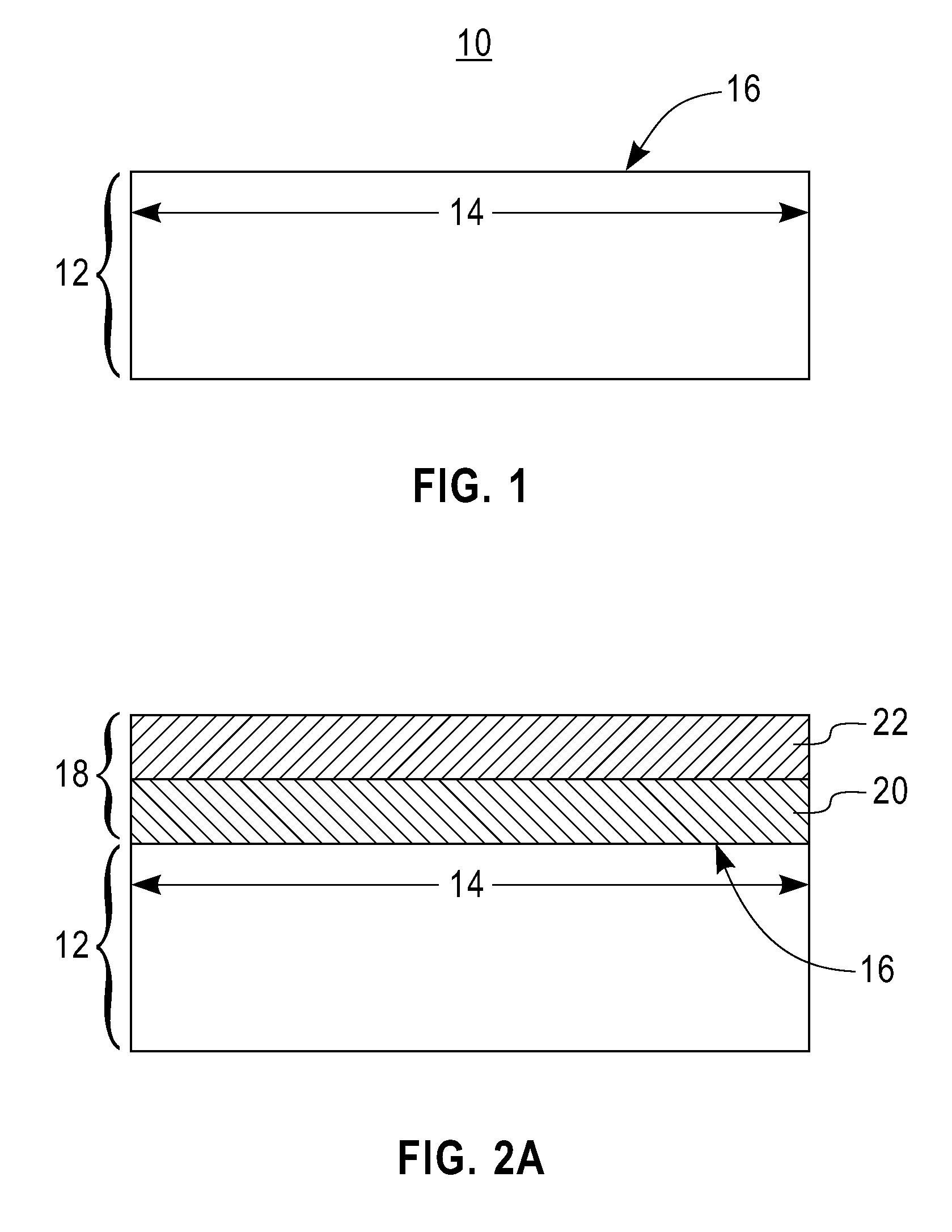
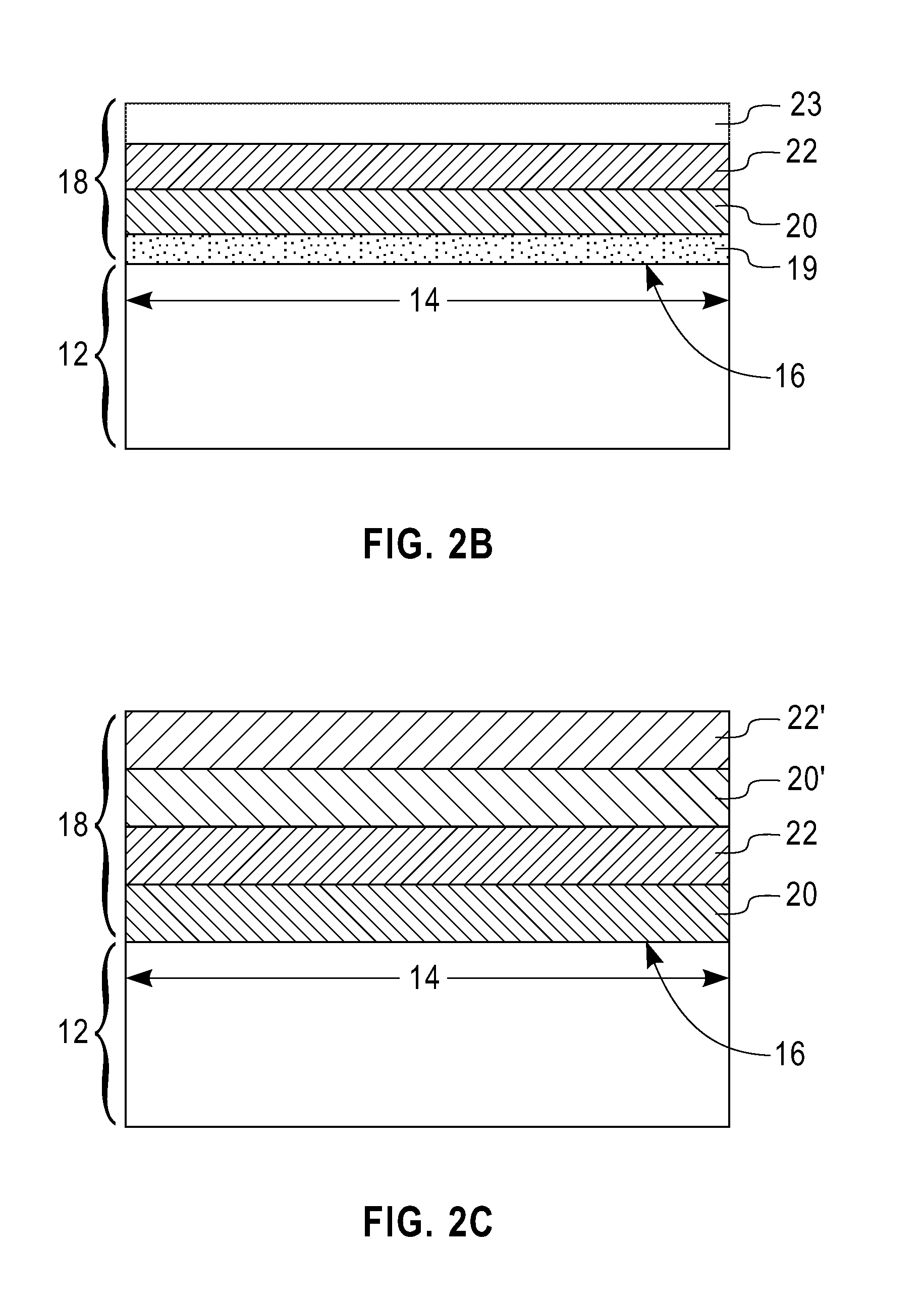
[0029]The present invention, which provides a simple and low cost method of fabricating SOI substrates that can be used in various semiconductor applications, including in solar cell or photovoltaic cell fabrication, will now be described in greater detail by referring to the following discussion and drawings that accompany the present application. It is noted that the drawings of the present application are provided for illustrative purposes only and, as such, the drawings are not drawn to scale.

[0030]In the following description, numerous specific details are set forth, such as particular structures, components, materials, dimensions, processing steps and techniques, in order to provide a thorough understanding of the present invention. However, it will be appreciated by one of ordinary skill in the art that the invention may be practiced without these specific details. In other instances, well-known structures or processing steps have not been described in detail in order to avoi...


PUM


Abstract

A lost cost method for fabricating SOI substrates is provided. The method includes forming a stack of p-type doped amorphous Si-containing layers on a semiconductor region of a substrate by utilizing an evaporation deposition process. A solid phase recrystallization step is then performed to convert the amorphous Si-containing layers within the stack into a stack of p-type doped single crystalline Si-containing layers. After recrystallization, the single crystalline Si-containing layers are subjected to anodization and at least an oxidation step to form an SOI substrate. Solar cells and/or other semiconductor devices can be formed on the upper surface of the inventive SOI substrate.

Description

FIELD OF THE INVENTION[0001]The present invention relates to semiconductor structures and a method of fabricating the same. More particularly, the present invention relates to a low cost semiconductor-on-insulator (SOI) substrate that can be used in a variety of semiconductor applications including, for example, as a substrate for a solar or photovoltaic cell. The present invention also provides a method of fabricating a solar cell utilizing the inventive SOI substrate as well as a solar cell including the same.BACKGROUND OF THE INVENTION[0002]A solar cell or photovoltaic cell is a device that converts sunlight directly into electricity by the photovoltaic effect. Sometimes the term “solar cell” is reserved for devices intended specifically to capture energy from sunlight, while the term “photovoltaic cell” is used when the source is unspecified. Assemblies of cells are used to make solar panels, solar modules, or photovoltaic arrays.[0003]The out voltage of a solar cell is limited ...

Claims


Application Information

Patent Timeline
IPC IPC(8): H01L31/0376H01L21/762
CPCH01L21/02529H01L21/02532H01L21/02573H01L21/02667H01L21/7624H01L31/046H01L21/76262H01L31/03921H01L31/1872Y02E10/50H01L21/76245H01L31/0463H01L31/0465Y02P70/50
Inventor BEDELL, STEPHEN W.DE SOUZA, JOEL P.FOGEL, KEITH E.HOVEL, HAROLD J.INNS, DANIEL A.KIM, JEEHWANSADANA, DEVENDRA K.SAENGER, KATHERINE L.SHAHIDI, GHAVAM G.
Owner GLOBALFOUNDRIES INC
Why Eureka
Try Eureka