

Semiconductor device
- Summary
- Abstract
- Description
- Claims
- Application Information
AI Technical Summary
Benefits of technology
Problems solved by technology
Method used
Image

Examples
first embodiment
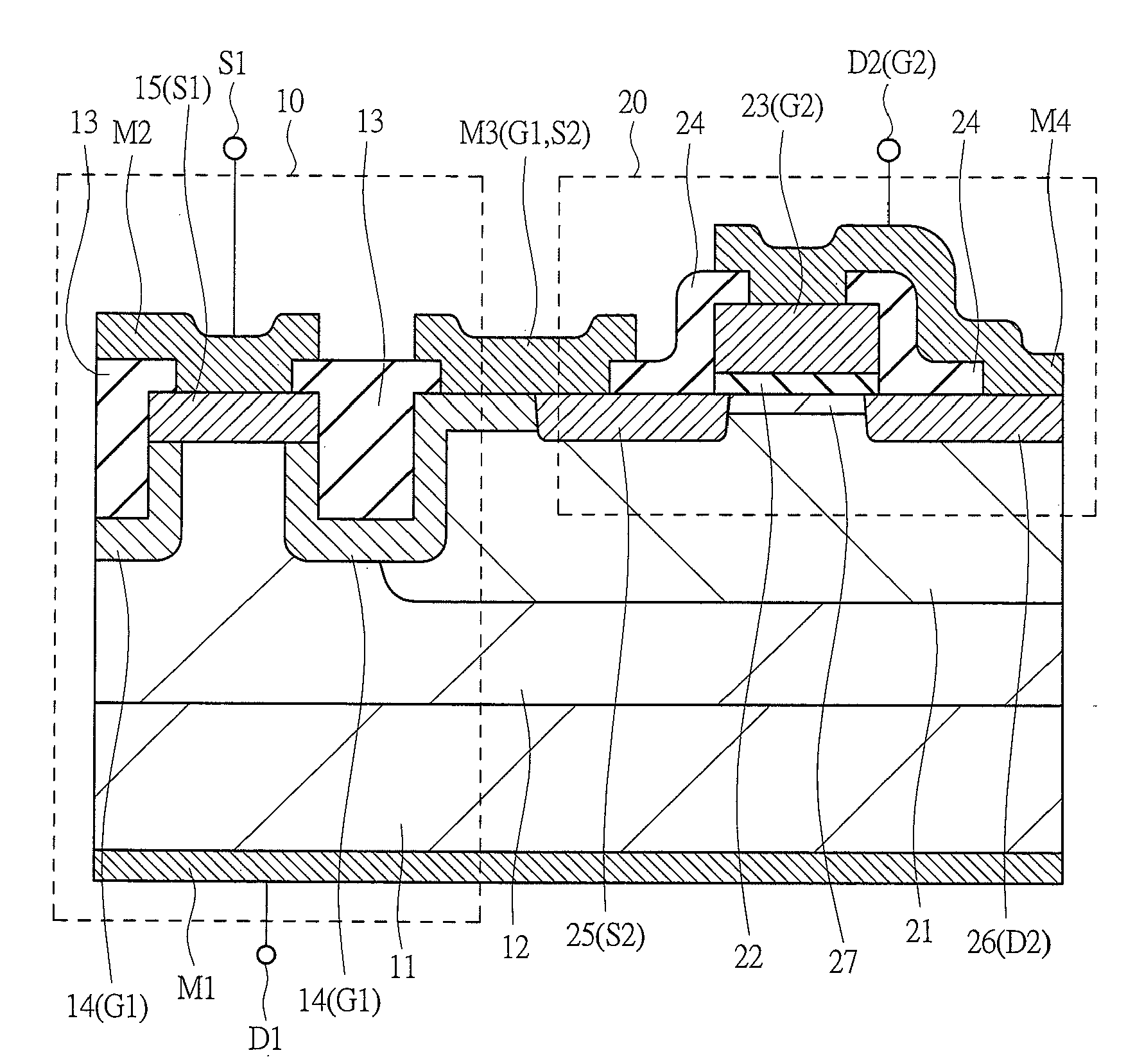
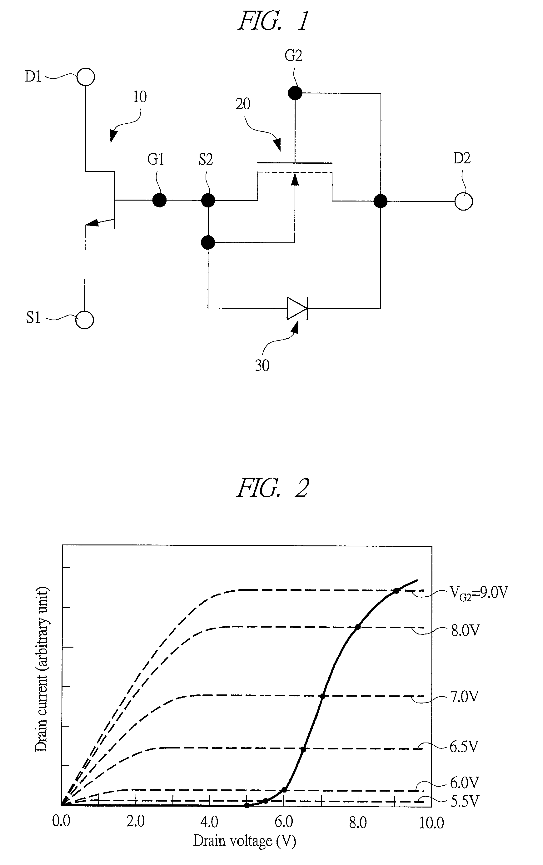
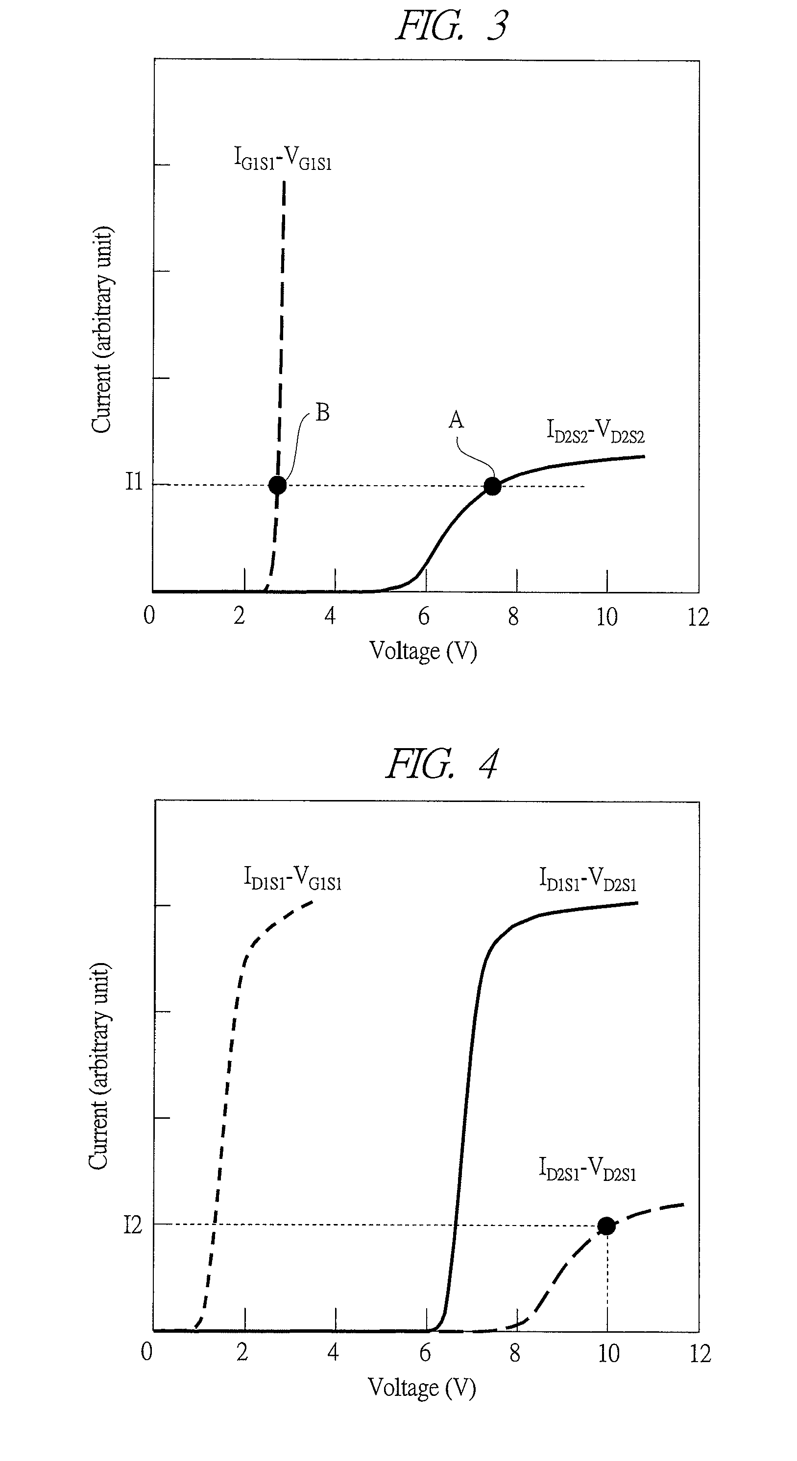
[0038]FIG. 1 illustrates a circuit diagram for describing a semiconductor device of a first embodiment. The semiconductor device of the first embodiment has a junction FET 10 as a main transistor. The junction FET 10 includes: a first gate electrode G1, which is a gate electrode; a first source electrode S1, which is a source electrode; and a first drain electrode D1, which is a drain electrode. The junction FET 10 of the first embodiment is an n-channel type, in which a drift layer serving as a channel is formed of an n-type semiconductor, a gate layer for generating a depletion layer in the drift layer is formed of a p-type semiconductor, and source / drain layers are formed of an n-type semiconductor. The junction FET 10 of the first embodiment is formed with using SiC as a base material.
[0039]Moreover, the semiconductor device of the first embodiment has a MISFET 20, which is a metal insulator semiconductor (MIS) type field effect transistor, as a transistor for control. The MISFE...
second embodiment
[0100]A semiconductor device of a second embodiment has a composite semiconductor device composed of the junction FET 10 and the MISFET 20 as described with reference to the circuit diagram of FIG. 1 described above in the same manner as the semiconductor device of the first embodiment.
[0101]A cross-sectional view of main parts of the semiconductor device of the second embodiment is illustrated in FIG. 17. In the semiconductor device of the second embodiment, the junction FET 10 and the MISFET 20 are formed on different semiconductor substrates (chips). The junction FET 10 is formed on a first semiconductor substrate 11a, and the MISFET 20 is formed on a second semiconductor substrate 11b. These two semiconductor substrates 11a and 11b are mounted on the same base plate 70 by solder-bonding. The two semiconductor substrates 11a and 11b are sealed in the same package. Hereinafter, the structure of the semiconductor device of the second embodiment will be described in more detail.
[010...
third embodiment
[0119]In a third embodiment, a semiconductor device in which semiconductor elements composed of the junction FET 10 and the MISFET 20 described in the first embodiment are used will be described. A circuit diagram of the semiconductor device of the third embodiment is shown in FIG. 20. The semiconductor device of the third embodiment has the junction FET 10 and the MISFET 20, which are composed of two independent individual semiconductor elements, as components thereof. In other words, the junction FET 10 and the MISFET 20 are composed of mutually-different packages. Terminals of the semiconductor elements such as the junction FET 10 and the MISFET 20 are disposed on the same circuit board (or printed circuit board) 60 and connected by wiring on the circuit board 60 so as to form the device.
[0120]FIG. 20 illustrates a boost chopper UC for a power factor improvement circuit (PFC). The boost chopper UC has the following components. Two diodes 31 and 32 are disposed on the circuit boar...
PUM
 Abstract
Description
Claims
Application Information