Transistor

Inactive Publication Date: 2018-08-23
NUVOTON
View PDF8 Cites 0 Cited by
  • Summary
  • Abstract
  • Description
  • Claims
  • Application Information

AI Technical Summary

Benefits of technology

The invention is about a transistor structure that uses a superlattice structure between the gate and barrier layer. This structure has a larger lattice constant than GaN, which helps to deplete the two-dimensional electron gas in the barrier layer and create a normally off transistor. As a result, the transistor has a higher threshold voltage, which solves the problem of low threshold voltage.

Problems solved by technology

Although the two-dimensional electron gas with high electron concentration and excellent transmission characteristics make the performance of output current density and on-resistance of the device extremely excellent, it causes the device to be in a normally on state, and a normally off (or enhancement mode) electronic device is not easily manufactured, resulting in many restrictions in the application.
However, for the use of the recessed gate, the fluoride ion processed gate and the thin InGaN depolarization layer, the threshold voltage thereof is still relatively unstable or still less than +1 volt.
However, in addition to the epitaxial growth is difficult, the increase of the threshold voltage is also quite limited.

Method used


Image

  • Transistor
  • Transistor
  • Transistor

Examples


Embodiment Construction

[0028]In the following detailed description, for purposes of explanation, numerous specific details are set forth in order to provide a thorough understanding of the disclosed embodiments. It will be apparent, however, that one or more embodiments may be practiced without these specific details. In other instances, well-known structures and devices are schematically shown in order to simplify the drawing.

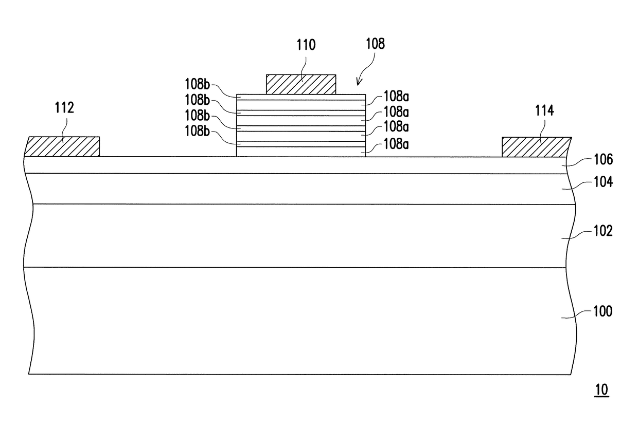
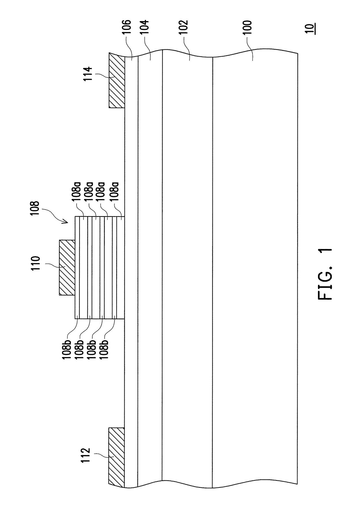
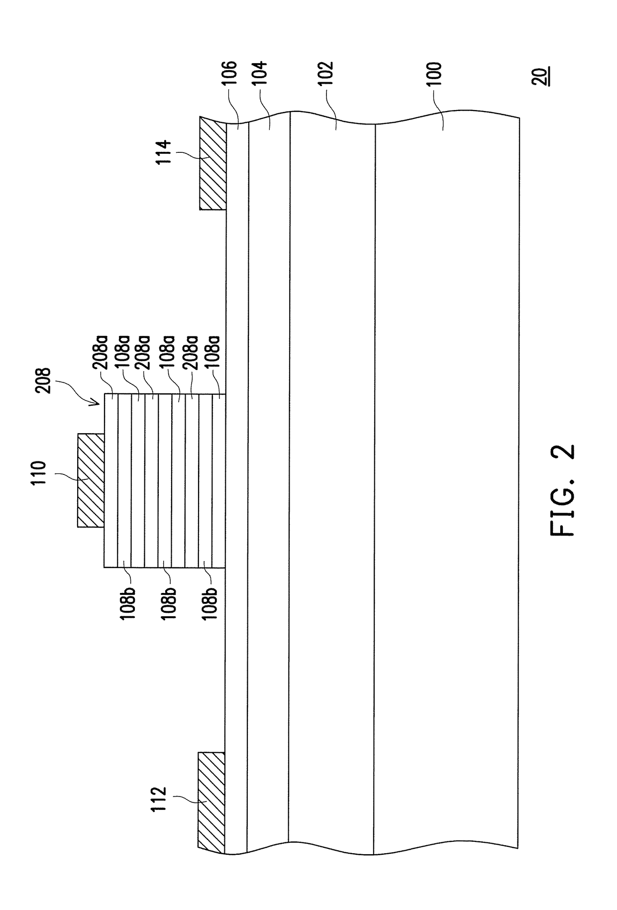
[0029]FIG. 1 is a schematic cross-sectional view illustrating a transistor according to an embodiment of the invention. Referring to FIG. 1, a transistor 10 includes a buffer layer 102, a channel layer 104, a barrier layer 106, a superlattice structure 108, a gate 110, a source 112 and a drain 114. In the embodiment, the superlattice structure 108 having a depolarization field is used to deplete the two-dimensional electron gas formed in the barrier layer 106, so as to form a normally off transistor. Additionally, by changing the thickness and composition of each layer in the superl...


PUM


Abstract

A transistor including a buffer layer, a channel layer, a barrier layer, a superlattice structure, a gate, a source and a drain is provided. The buffer layer, the channel layer, the barrier layer, the superlattice structure and the gate are sequentially disposed on a substrate. The source and drain are disposed on the barrier layer and respectively at two sides of the superlattice structure, or on the channel layer and respectively at two sides of the barrier layer. The superlattice structure includes at least one first metal nitride layer and at least one second metal nitride layer stacked to each other. The average lattice constant of the superlattice structure is greater than that of GaN. The metal of each of the first and second metal nitride layers is at least one selected from the group consisting of Al, Ga and In. The first and second metal nitride layers are different.

Description

CROSS-REFERENCE TO RELATED APPLICATION[0001]This application claims the priority benefit of Taiwan application serial no. 106105541, filed on Feb. 20, 2017. The entirety of the above-mentioned patent application is hereby incorporated by reference herein and made a part of this specification.BACKGROUND OF THE INVENTIONField of the Invention[0002]The invention relates to a semiconductor device, and particularly relates to a transistor.Description of Related Art[0003]For a GaN-based transistor, since its advantages of high electron mobility, high voltage resistance, low channel resistance and fast switching, it has been gradually applied to power devices. In a nitride material containing Group III elements, due to the uneven distribution of electrons, a spontaneous polarization field will be generated on a c-axis. Additionally, between heterogeneous materials, energy band discontinuity and lattice constant mismatch will generate a piezoelectric polarization field. Thus, electrons are ...

Claims


Application Information

Patent Timeline
IPC IPC(8): H01L29/15H01L29/10H01L29/66H01L29/778H01L21/02
CPCH01L29/155H01L29/1075H01L29/66462H01L29/7783H01L21/02507H01L21/02241H01L29/2003B82Y40/00H01L29/42364H01L29/7787H01L21/02458H01L29/432H01L29/7786
Inventor TSAI, JUNG-TSELIN, HENG-KUANG
Owner NUVOTON
Why Eureka
Try Eureka