Semiconductor device

Inactive Publication Date: 2010-09-09
SEIKO INSTR INC
View PDF6 Cites 1 Cited by
  • Summary
  • Abstract
  • Description
  • Claims
  • Application Information

AI Technical Summary

Benefits of technology

[0017]According to the present invention, the N-channel high-voltage MOS transistor is configured such that the wiring metal connected to the drain region is laid above the boundary portion between the oxide film formed by LOCOS process or the like of the low impurity concentration region and the high impurity concentration region forming the drain region. Accordingly, an electric field concentration at the boundary portion which is the

Problems solved by technology

In general, in a case where the high-voltage NMOS is less frequently used in the semiconductor integrated circuit, limitations are imposed on the high-voltage NMOS in terms of structure for reducing cost as described above, and the element has to be designed under the limiting conditions.
However, in the high-voltage MOS transistor

Method used


Image

  • Semiconductor device
  • Semiconductor device
  • Semiconductor device

Examples


Example

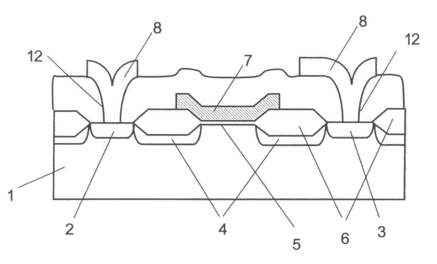
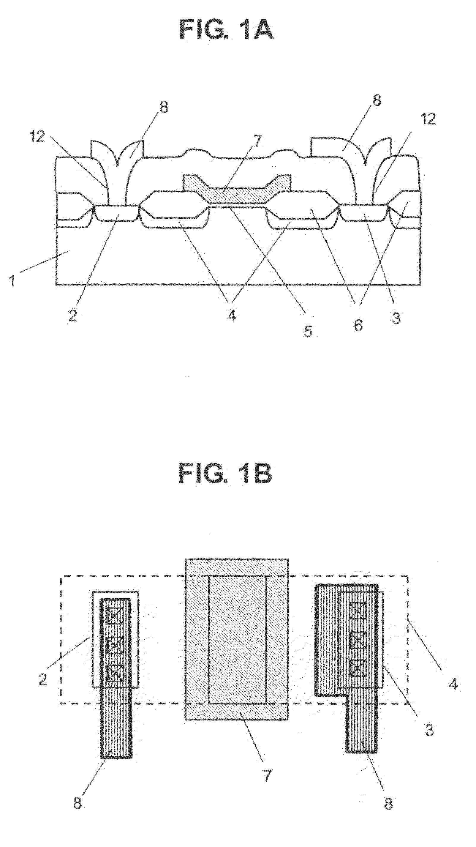
[0029]Hereinafter, an embodiment of the present invention is described with reference to the drawings.

[0030]FIGS. 1A and 1B are a schematic cross-sectional view and a schematic plan view, respectively, each illustrating a high-voltage N-channel metal oxide semiconductor (NMOS) transistor according to the embodiment of the present invention. The high-voltage NMOS transistor includes a gate insulating film 5 formed on a surface of a P-type semiconductor substrate 1 or P-type well, a LOCOS oxide film 6 which is an insulating film formed contiguously to the gate insulating film 5 and has a thickness larger than that of the gate insulating film, a gate electrode 7 formed so as to extend across the gate insulating film 5 and portions of the LOCOS oxide film 6 close to the gate insulating film, an N-type low impurity concentration region 4 formed below the LOCOS oxide film 6, N-type high impurity concentration regions 2 and 3, each formed next to the N-type low impurity concentration regio...


PUM


Abstract

Provided is a semiconductor device including an N-channel high-voltage MOS transistor, in which wiring metal connected to a drain region is laid above a boundary portion between an oxide film formed by LOCOS process or the like on a low impurity concentration region and a high impurity concentration region forming the drain region, to thereby alleviate an electric field concentration at the boundary portion which is a contact portion between the low impurity concentration region and the high impurity concentration region by an electric field generated from the wiring metal toward a semiconductor substrate.

Description

BACKGROUND OF THE INVENTION[0001]1. Field of the Invention[0002]The present invention relates to a semiconductor device including a semiconductor element such as an N-channel high-voltage metal oxide semiconductor (MOS) transistor.[0003]2. Description of the Related Art[0004]Elements used in a semiconductor device include a low-voltage element which has a low operating voltage, and a high-voltage element which may be used even when a power supply voltage is high, depending on the respective use thereof. For example, a high-voltage element is used only in a section which directly handles a voltage applied to and output from the semiconductor device, while a low-voltage element is used in a section which performs internal signal processing. The low-voltage element occupies a smaller area than the high-voltage element. Accordingly, the high-voltage element is used only in a section which determines the performance specification of the integrated circuit and is difficult to modify, such...

Claims


Application Information

Patent Timeline
IPC IPC(8): H01L29/78
CPCH01L23/485H01L29/0653H01L29/402H01L29/41725H01L2924/0002H01L2924/00H01L2924/13091
Inventor HASEGAWA, HISASHIYOSHINO, HIDEO
Owner SEIKO INSTR INC
Why Eureka
Try Eureka