

Semiconductor Nanocrystal Synthesis Using a Catalyst Assisted Two-phase Reaction
a technology of semiconductor and nanocrystal, which is applied in the direction of selenium/tellurium compunds, chemistry apparatus and processes, thermoelectric devices, etc., can solve the problem of reducing the quantum yield of the nanocrystal
- Summary
- Abstract
- Description
- Claims
- Application Information
AI Technical Summary
Problems solved by technology
Method used
Image

Examples
example
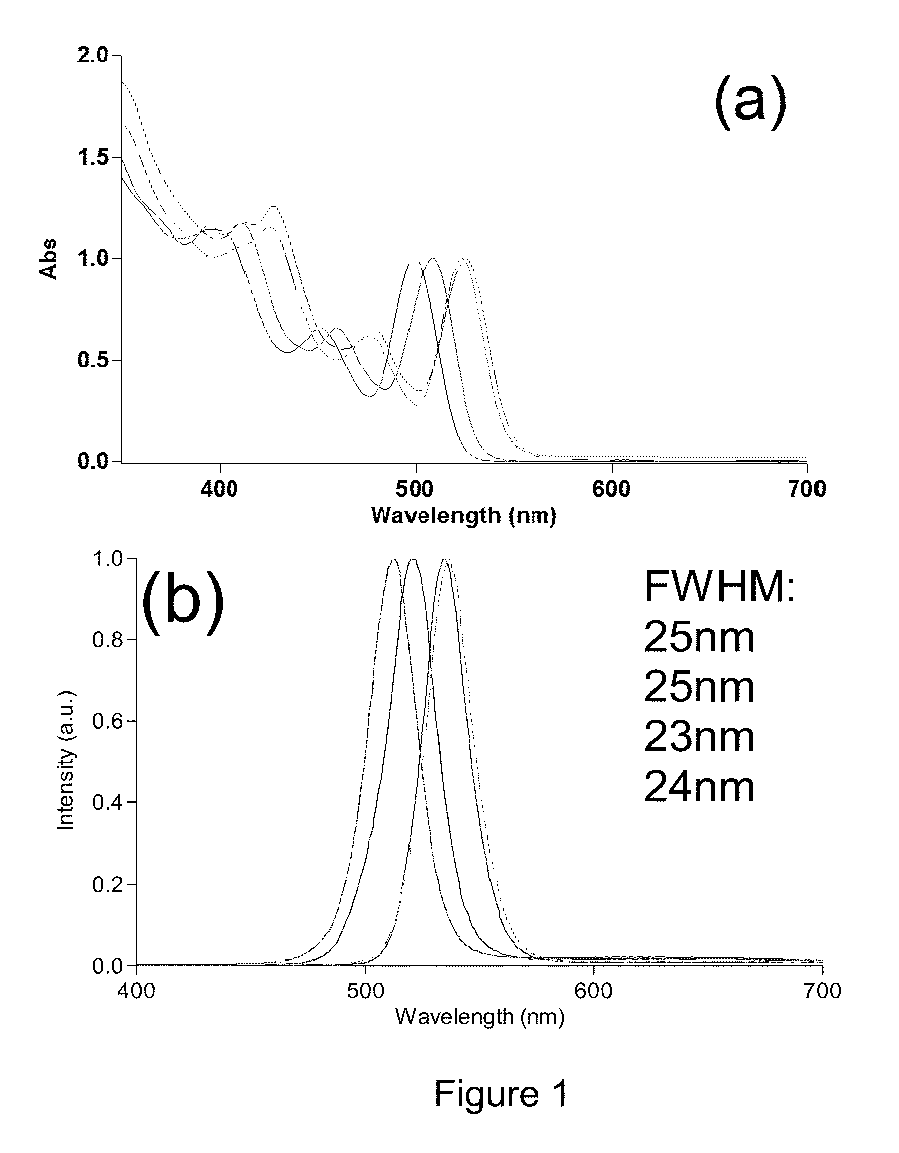
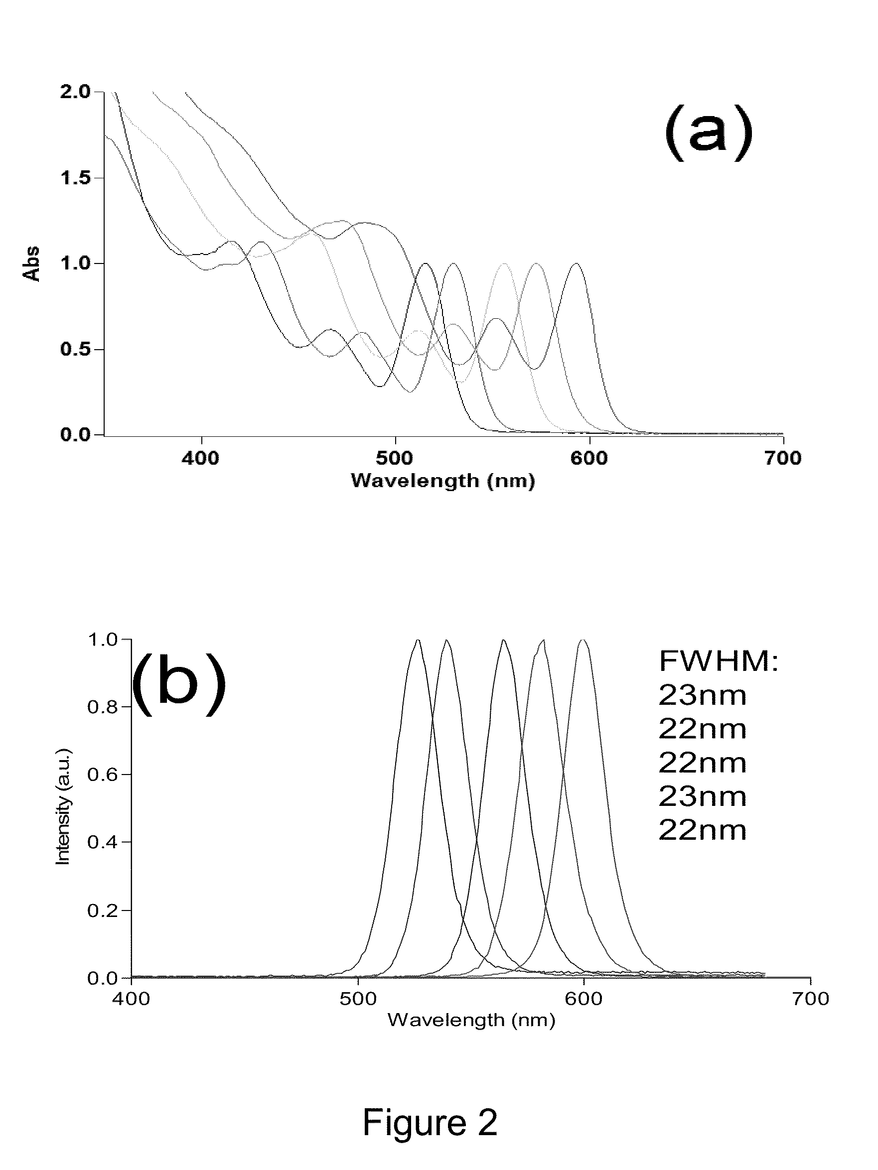
[0014]Preparing a batch of high quality (3 nm) II-VI Semiconductor Nanocrystals
[0015]The present example discloses how to prepare stable, high quality (3 nm) cadmium selenide (CdSe) semiconductor nanocrystals.
[0016]First, 61.632 grams of solid cadmium oxide (CdO(s)), 189.82 grams of oleic acid (technical grade), and 210 grams of octadecene (ODE) are loaded into a 1-liter reaction flask. The system is purged with a nitrogen flow for 10 minutes.
[0017]While the reaction flask is purging, two separate stock solutions are made in a nitrogen flowing glove box. Stock Solution 1 contains 15.8 grams of 20% Se:TBP (selenium dissolved in tributylphosphine) solution and 84.2 grams of ODE. Stock Solution 2 contains 4.74 grams of 20% Se:TBP solution and 45.4 grams of ODE. The stock solutions are transported out of the glove box while sealed from the air and loaded separately into syringe 1 and 2, respectively, under nitrogen. It is important that the solutions are not exposed to oxygen in the air...
PUM
 Abstract
Description
Claims
Application Information