

Iii nitride electronic device and iii nitride semiconductor epitaxial substrate
- Summary
- Abstract
- Description
- Claims
- Application Information
AI Technical Summary
Benefits of technology
Problems solved by technology
Method used
Image

Examples
experiment 1
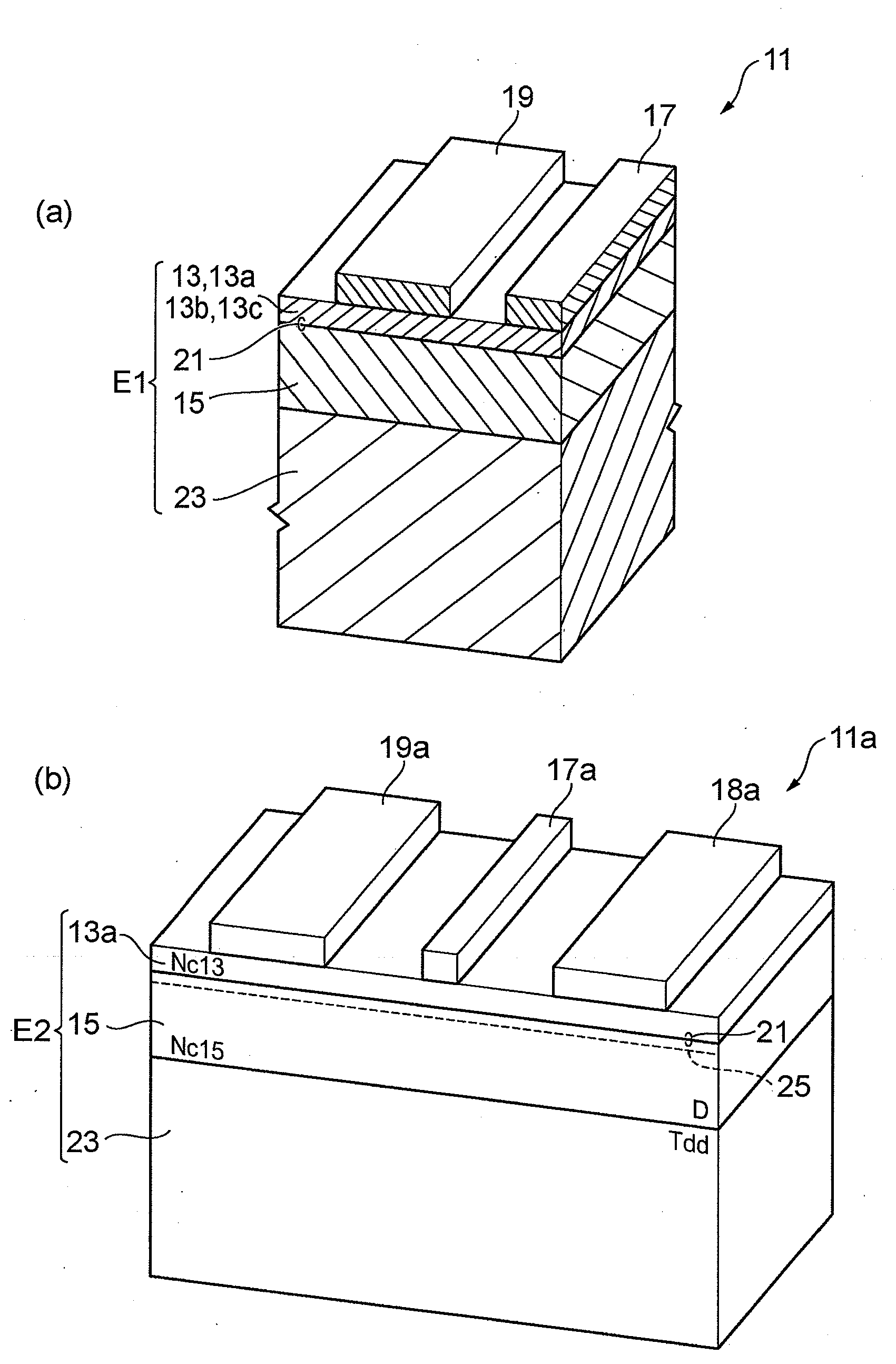
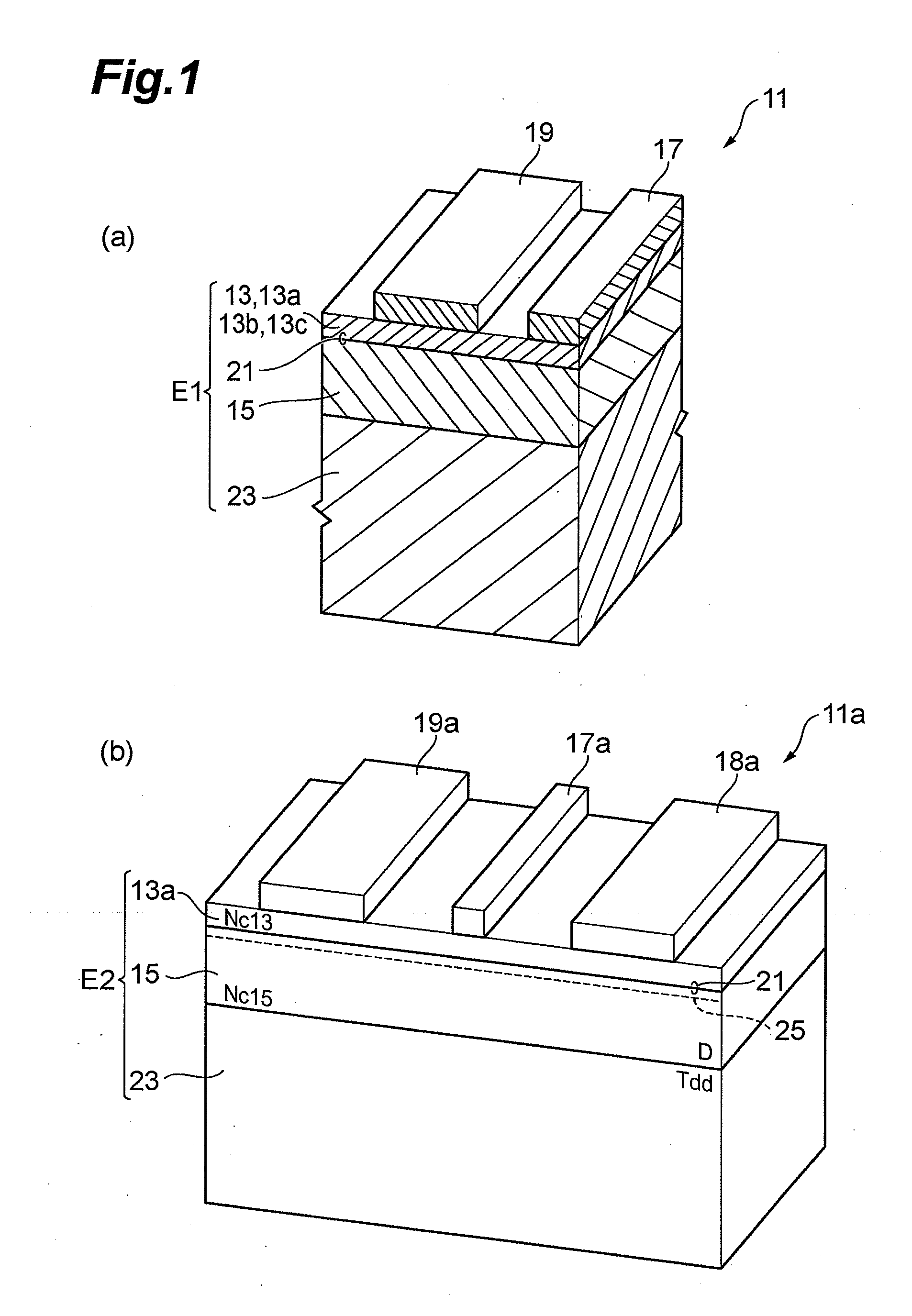
[0066]An epitaxial substrate was fabricated on a (0001) sapphire substrate by metal organic vapor phase epitaxy (MOVPE) as follows. The substrate was heat-treated in a hydrogen atmosphere at a temperature of 1050° C. under a reactor pressure of 100 torr (1 torr corresponds to 133.322 Pa) for 5 minutes. After this treatment, a low-temperature GaN buffer layer (25 nm) is grown at a temperature of 520° C. Then, an undoped 2-μm GaN layer was grown at a temperature of 1050° C. under a reactor pressure of 100 torr with V / III=1000. Then, an undoped Al0.25Ga0.75N layer was grown at a temperature of 1070° C. under a reactor pressure of 50 torr with V / III=500. These processes produced an epitaxial substrate A-1. The threading dislocation density in the GaN layer was 2×109 cm−2, which was evaluated through TEM.
experiment 2
[0067]An epitaxial substrate was fabricated on a 6H-SiC substrate by MOVPE as follows. The substrate was heat-treated in a hydrogen atmosphere at a temperature of 1050° C. under a reactor pressure of 100 torr for 5 minutes. After this treatment, an undoped Al0.5Ga0.5N buffer layer (100 nm) was grown at a temperature of 1080° C. Then, a 2-μm undoped GaN layer was grown at a temperature of 1050° C. under a reactor pressure of 100 torr with V / III=1000. Then, a 25-nm undoped Al0.25Ga0.75N layer was grown at a temperature of 1070° C. under a reactor pressure of 50 torr with V / III=500. These processes produced an epitaxial substrate B-1. The dislocation density in the GaN layer was 5×108 cm−2, which was evaluated through TEM.
experiment 3
[0068]An epitaxial substrate 31 as shown in FIG. 3 was fabricated by MOVPE as follows. A high-resistance GaN substrate 33 was treated in an ammonia atmosphere at a temperature of 1000° C. for 5 minutes. After this treatment, a 2-μm undoped GaN layer 35 was grown at a temperature of 1050° C. under a reactor pressure of 100 torr with V / III=1000. Then, a 25-nm undoped Al0.25Ga0.75N layer 37 was grown at a temperature of 1070° C. under a reactor pressure of 50 torr with V / III=500. These processes produced epitaxial substrates C-1 and D-1. The dislocation density in the GaN layer of the epitaxial substrate C-1 was 1×108 cm−2, and the dislocation density in the GaN layer of the epitaxial substrate D-1 was 5×106 cm−2, which were evaluated through TEM.
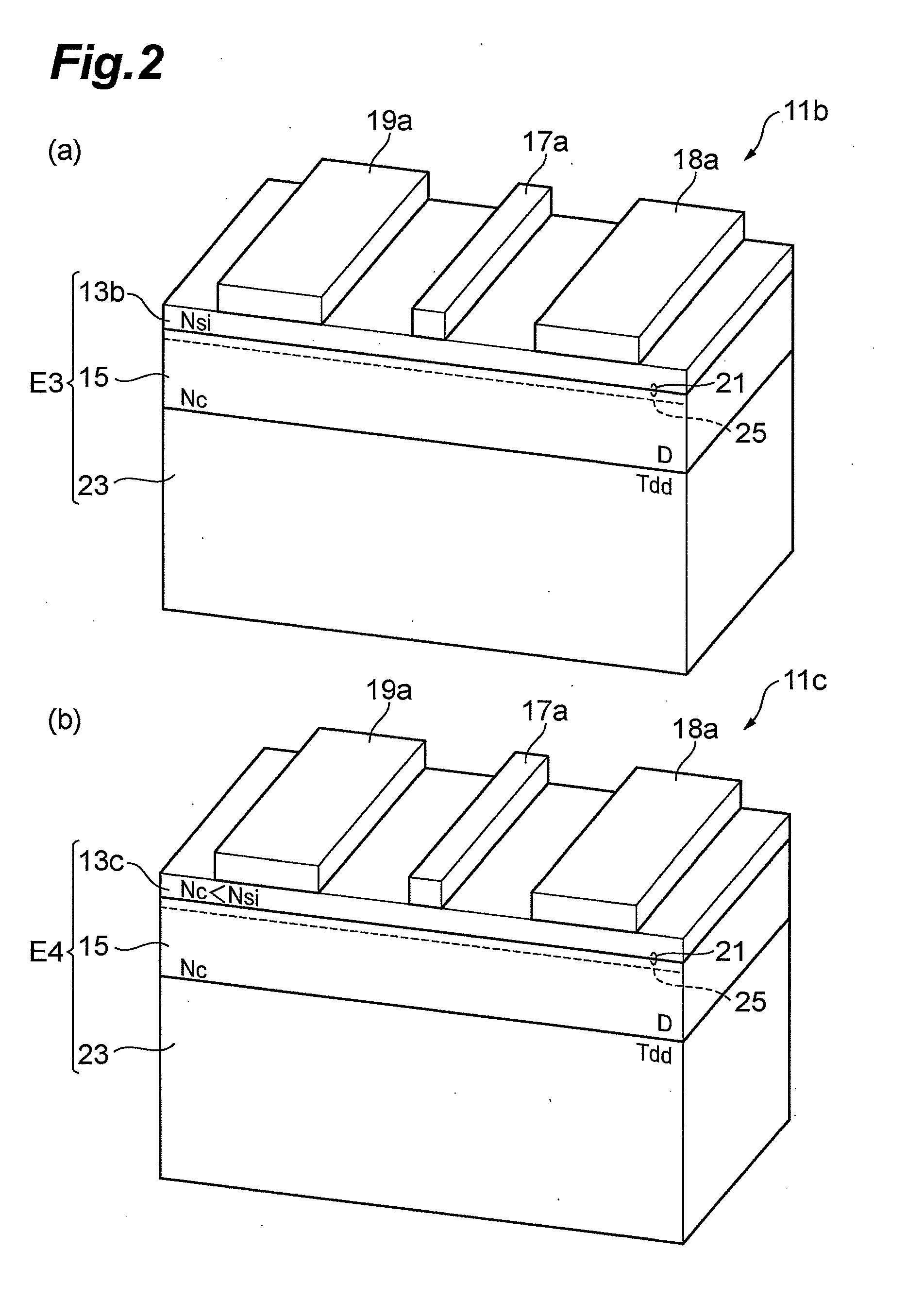
[0069]AlGaN layers were grown under various growth pressures as in the experiments described above. Epitaxial wafers A-2 through E-2 were fabricated under a growth pressure of 75 torr. Epitaxial wafers A-3 through E-3 were fabricated under a g...
PUM
 Abstract
Description
Claims
Application Information