Semiconductor storage device

a storage device and semiconductor technology, applied in the field of semiconductor storage devices, can solve the problems of increasing the difficulty of exposure, unable to conduct exposure and processing on the memory cell array and the peripheral circuit collectively, and more difficult to form contact holes by using photolithography than to form interconnections

Active Publication Date: 2010-09-16
KIOXIA CORP
View PDF4 Cites 2 Cited by
  • Summary
  • Abstract
  • Description
  • Claims
  • Application Information

AI Technical Summary

Benefits of technology

[0015]a memory cell array including memory cell transistor from which data depending upon a value of a retained threshold voltage can be read out by applying a...

Problems solved by technology

In general, it is more difficult to form contact holes by using photolithography than to form interconnections (see, for example, Japanese Patent Laid-Open No. 2004-348118).
As the size shrinking of the non-volatile semiconductor memory is advanced, the lithography margin and processing margin cannot be ensured, and consequently it is not possible to condu...

Method used


Image

  • Semiconductor storage device
  • Semiconductor storage device
  • Semiconductor storage device

Examples


first embodiment

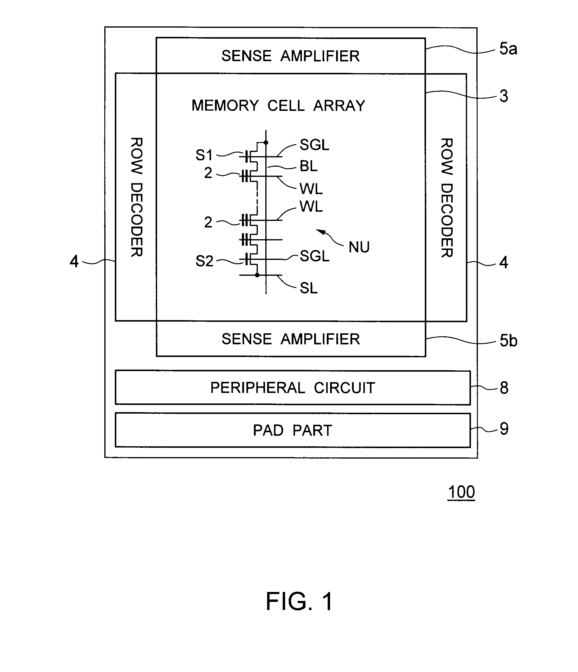
[0054]FIG. 1 is a block diagram showing an example of a NAND flash memory 100 including sense amplifiers according to a first embodiment which is a mode of the present invention.

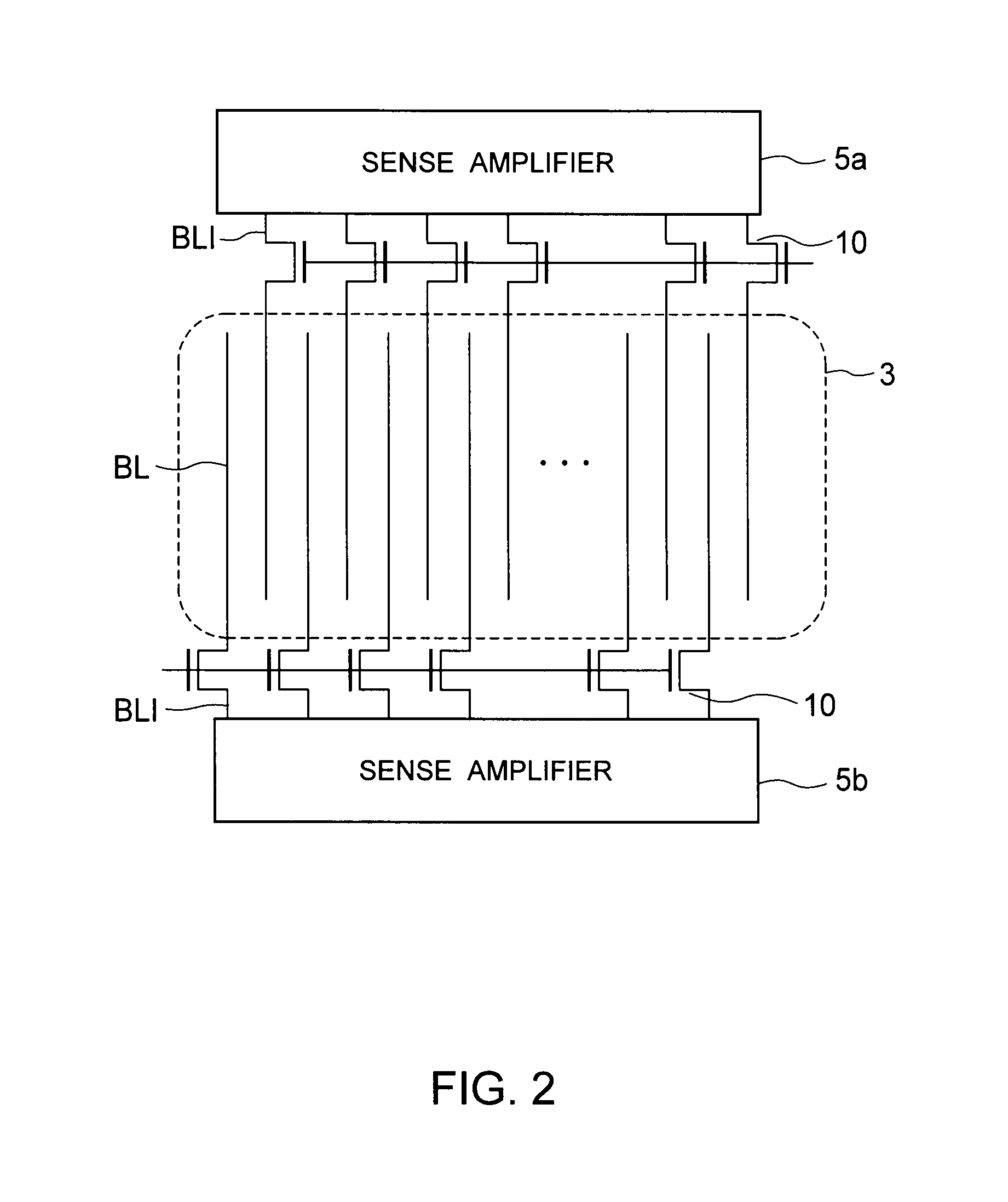
[0055]As shown in FIG. 1, the NAND flash memory 100 according to the present embodiment includes a memory cell array 3 having memory cell transistors 2 arranged in a matrix form, row decoders 4, sense amplifiers 5a and 5b, a peripheral circuit 8, and a pad part 9.

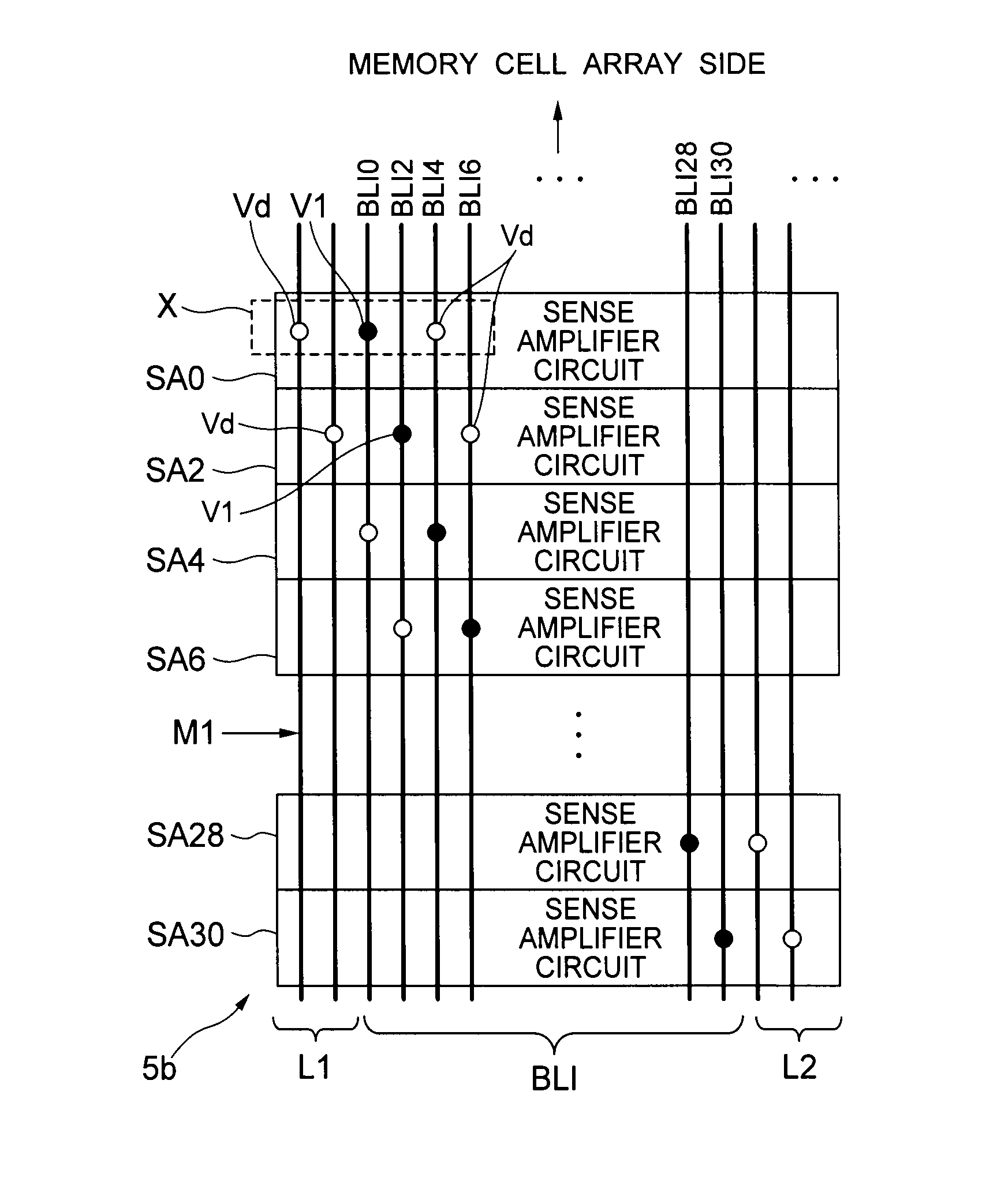
[0056]The memory cell array 3 is formed by arranging a plurality of NAND cell units NU each of which is obtained by connecting memory cell transistors 2 in series. The sense amplifiers 5a and 5b are arranged in the direction of the bit line BL of the memory cell array 3. The row decoders 4 are arranged respectively at both ends of the memory cell array 3 in the direction of the word line WL.

[0057]Each of the memory cell transistors 2 has, for example, a floating gate formed over a semiconductor substrate via a tunnel insulation film and a control ga...


PUM


Abstract

A semiconductor storage device has a sense amplifier. The sense amplifier includes a first lower interconnection; a second interlayer insulation film formed on the first interlayer insulation film and top of the first interconnection; a contact interconnection formed in a direction perpendicular to a substrate plane of the semiconductor substrate so as to pass through the second interlayer insulation film, and connected to the first lower interconnection; a first upper interconnection formed on the second interlayer insulation film and connected to the contact interconnection disposed under the first upper interconnection; a dummy contact interconnection formed in a direction perpendicular to the substrate plane of the semiconductor substrate in the second interlayer insulation film, and adjacent to the contact interconnection; and a second upper interconnection formed on the second interlayer insulation film so as to extend in the first direction, and connected to the dummy contact interconnection disposed under the second upper interconnection.

Description

CROSS-REFERENCE TO RELATED APPLICATION[0001]This application is based upon and claims the benefit of priority from the prior Japanese Patent Application No. 2009-62577, filed on Mar. 16, 2009, the entire contents of which are incorporated herein by reference.BACKGROUND OF THE INVENTION[0002]1. Field of the Invention[0003]The present invention relates to a semiconductor storage device including a plurality of interconnection layers which are connected by contact hole interconnections.[0004]2. Background Art[0005]In recent years, demands for small-sized large-capacity non-volatile semiconductor storage devices have increased rapidly. Among them, NAND flash memories which can be anticipated to have higher integration and larger capacities as compared with conventional NOR flash memories are attracting attention. The width and spacing (line and space) of interconnections in non-volatile semiconductor storage devices such as NAND flash memories are shrunk as the fine resolution technique...

Claims


Application Information

Patent Timeline
IPC IPC(8): G11C16/04G11C11/34G03F1/00G03F1/70H01L21/336H01L21/8247H01L27/10H01L27/115H01L29/788H01L29/792
CPCG11C8/10G11C16/26H01L27/11526H01L27/11521H01L27/11524H01L27/11519H10B41/10H10B41/35H10B41/40H10B41/30
Inventor SUZUKI, YUYAHISADA, TOSHIKIHOSOMURA, YOSHIKAZU
Owner KIOXIA CORP
Why Eureka
Try Eureka