Chemical sensor element, sensing apparatus, and sensing method

a sensor element and sensing technology, applied in the field of chemical sensors, can solve the problems and not achieving the effect of the proposed structure, so as to achieve the effect of increasing the shift of the resonance spectrum and reducing the width of the resonance spectrum

Inactive Publication Date: 2010-09-16
CANON KK
View PDF14 Cites 25 Cited by
  • Summary
  • Abstract
  • Description
  • Claims
  • Application Information

AI Technical Summary

Benefits of technology

[0010]The present invention intends to solve the above-mentioned problems, and intends to provide a chemical sensor element having a resonator construction which enables decrease of the width of the resonance spectrum and increase of the shift of the resonance spectrum for high-sensitive measurement.

Problems solved by technology

The above prior art techniques are not sufficient in the measurement sensitivity for high-sensitive detection of a low concentration of a target substance.
However, the proposed structures do not achieve any of the effects of decrease of the width of the resonance spectrum and increase of the shift of the resonance spectrum.

Method used


Image

  • Chemical sensor element, sensing apparatus, and sensing method
  • Chemical sensor element, sensing apparatus, and sensing method
  • Chemical sensor element, sensing apparatus, and sensing method

Examples


example 1

[0087]A sensor of Example 1 of the present invention is described below.

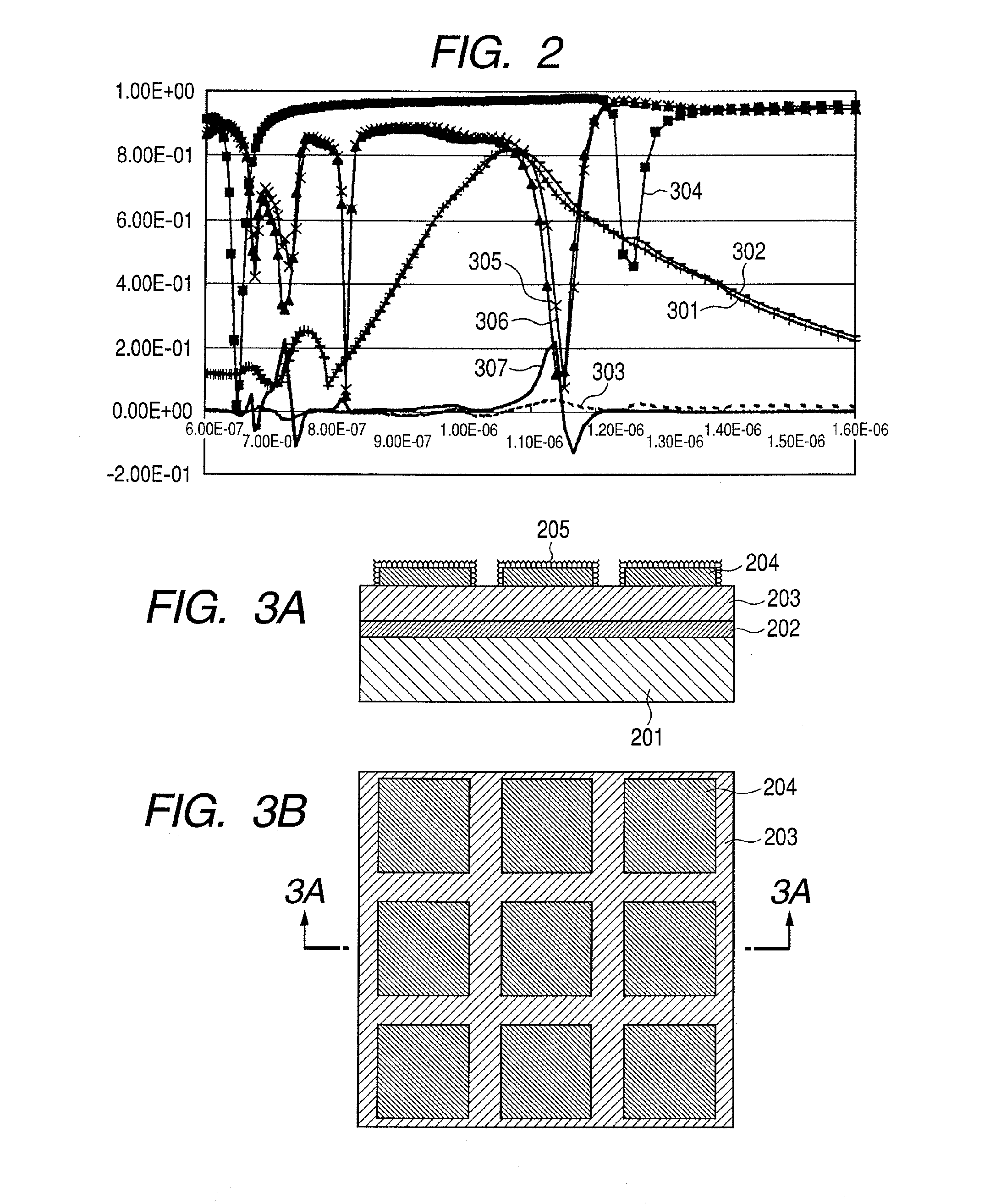
[0088]Firstly, a process for production of the sensor element of the present invention is described. FIGS. 4A-4D illustrate steps of production of the sensor element of this Example.

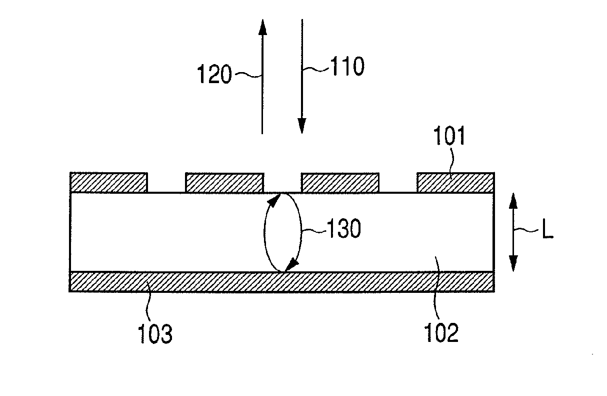
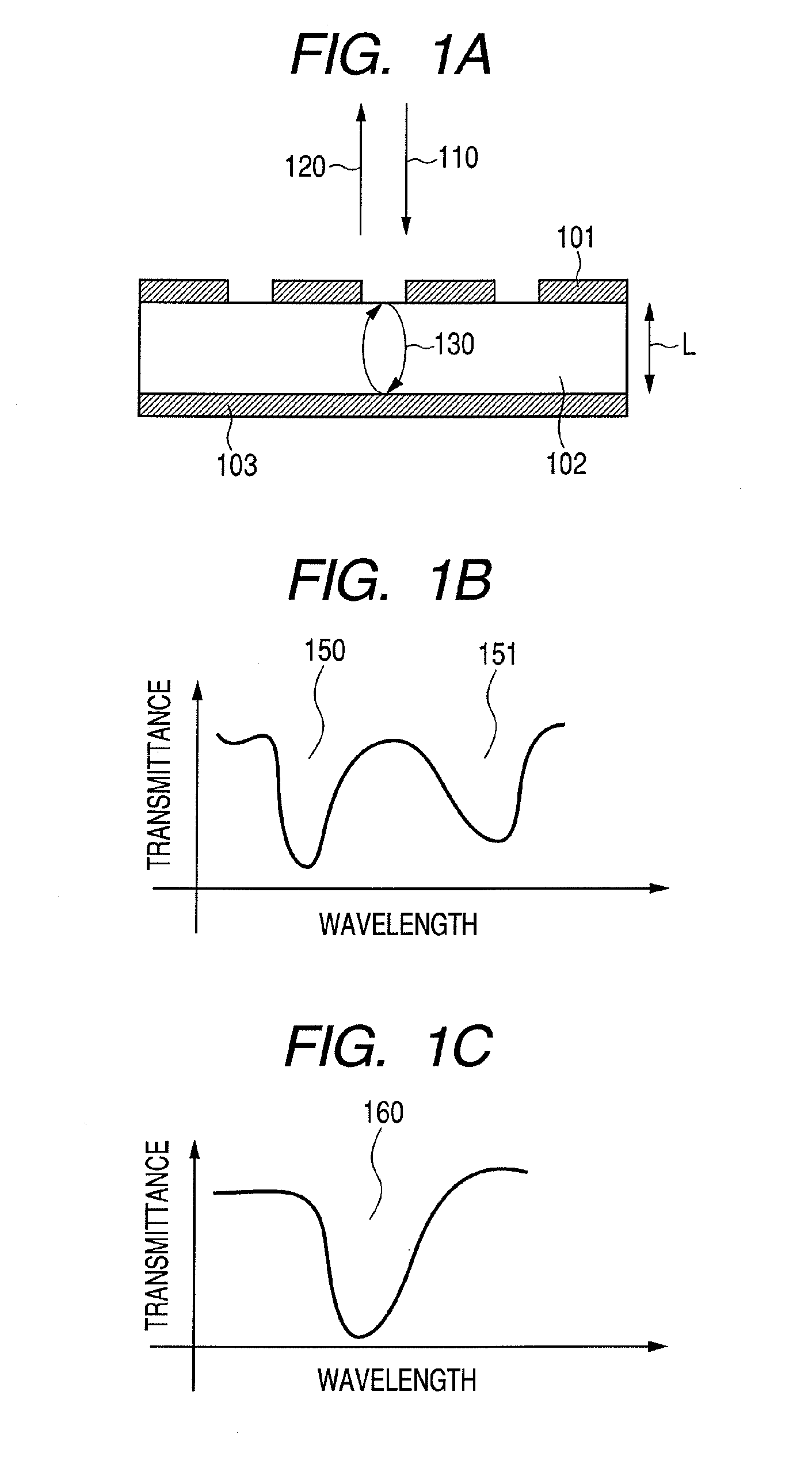
[0089]A quartz plate is used as the base plate 401, having a thickness of 525 μm. The thickness of quartz base plate 401 is not limited thereto.

[0090]As illustrated in FIG. 4A, a Au thin film is formed, on quartz base plate 401, as metal layer 402 in a thickness of about 100 nm by vapor deposition. The material of metal layer 402 is not limited to Au, but may be any metal which has a high reflectivity in the measurement wavelength range of the sensor element of this Example. Specifically, the material of metal layer 402 includes gold, silver, copper, platinum, and aluminum. The method of film formation is not limited to vapor deposition, but may be sputtering.

[0091]On the formed metal layer 402, a silicon dioxide film is formed as re...

example 2

[0113]A sensor element of Example 2 of the present invention is described below.

[0114]Firstly, a process for producing the sensor element of this Example is described. FIGS. 7A to 7D illustrate the sequence of the steps of production of the sensor element of this Example.

[0115]Quartz base plate 701 is provided, having a thickness of 525 μm. The thickness of quartz base plate 701 is not limited thereto.

[0116]As illustrated in FIG. 7A, on the surface of quartz base plate 701, a Au thin film is formed as metal layer 702 in a thickness of about 100 nm by vapor deposition. The material of metal layer 702 is not limited to Au, but may be any metal which has a high reflectivity in the measurement wavelength range of the sensor element of this Example. Specifically, the material of metal layer 702 includes gold, silver, copper, platinum, and aluminum. The method of formation of metal film 702 is not limited to vapor deposition, but may be sputtering.

[0117]On the formed metal layer 702, a si...


PUM

PropertyMeasurementUnit
resonance wavelengthaaaaaaaaaa
thicknessaaaaaaaaaa
surface plasmon resonance wavelengthaaaaaaaaaa

Abstract

A chemical sensor element contains a resonator having a first reflector in which particles of a fine metal structure are arranged two-dimensionally and periodically is counterposed with interposition of a dielectric layer to a second reflector, wherein the resonance wavelength of a resonator in which the entire of the first reflector is replaced by a metal thin film having the same thickness as the metal fine structure is different from the surface plasmon resonance wavelength induced in the metal fine structure; and the mode of the surface plasmon resonance excited in the metal fine structure is coupled with the mode of the resonator in which the entire of the first reflector is replaced by the metal thin film.

Description

TECHNICAL FIELD[0001]The present invention relates to a chemical sensor, particularly to a chemical sensor for detecting, from a change in an optical spectrum, a change in a dielectric constant caused by an antigen-antibody reaction on the surface of the sensor element. The present invention relates also to a sensing apparatus and sensing method employing the sensor.BACKGROUND ART[0002]A localized surface plasmon resonance (LSPR) can be induced in an electroconductive fine structure. Resonance conditions of the LSPR depend on the refractive index and dielectric constant surrounding the electroconductive structure. Therefore, a change in the dielectric constant around the electroconductive structure can be detected by a change in the resonance conditions. The change in the resonance conditions can be detected by measuring a change in the optical spectrum of the light beam projected to and transmitted through the electroconductive structure.[0003]The LSPR is sensitive to a change in t...

Claims


Application Information

Patent Timeline
Patent Type & Authority Applications(United States)
IPC IPC(8): G01N33/553G01N21/00G01N21/27G01N21/41
CPCG01N21/554G01N21/27Y10S436/805
Inventor YAMADA, TOMOHIROHANDA, YOICHIRO
Owner CANON KK
Why Eureka
Try Eureka