Photosensor and method of manufacturing the same
a technology of photosensors and manufacturing methods, applied in the field of photosensors, can solve the problems of low spatial resolution, limited upsizing, lack of immediacy, etc., and achieve the effect of suppressing the increase of leakage curren
- Summary
- Abstract
- Description
- Claims
- Application Information
AI Technical Summary
Benefits of technology
Problems solved by technology
Method used
Image

Examples
first exemplary embodiment
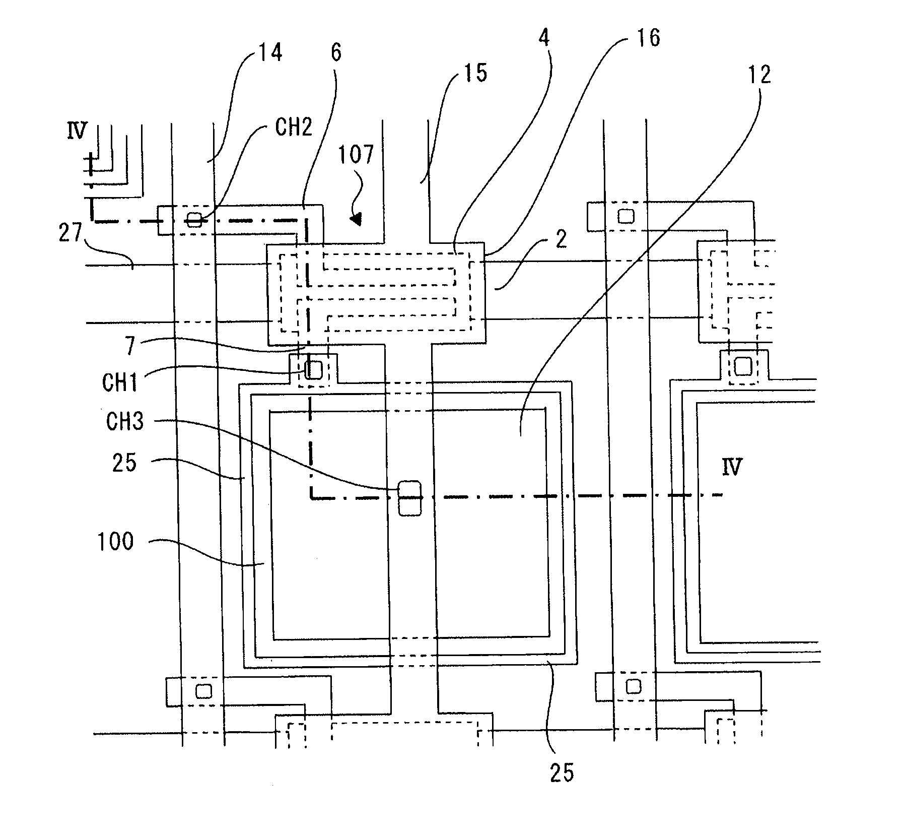
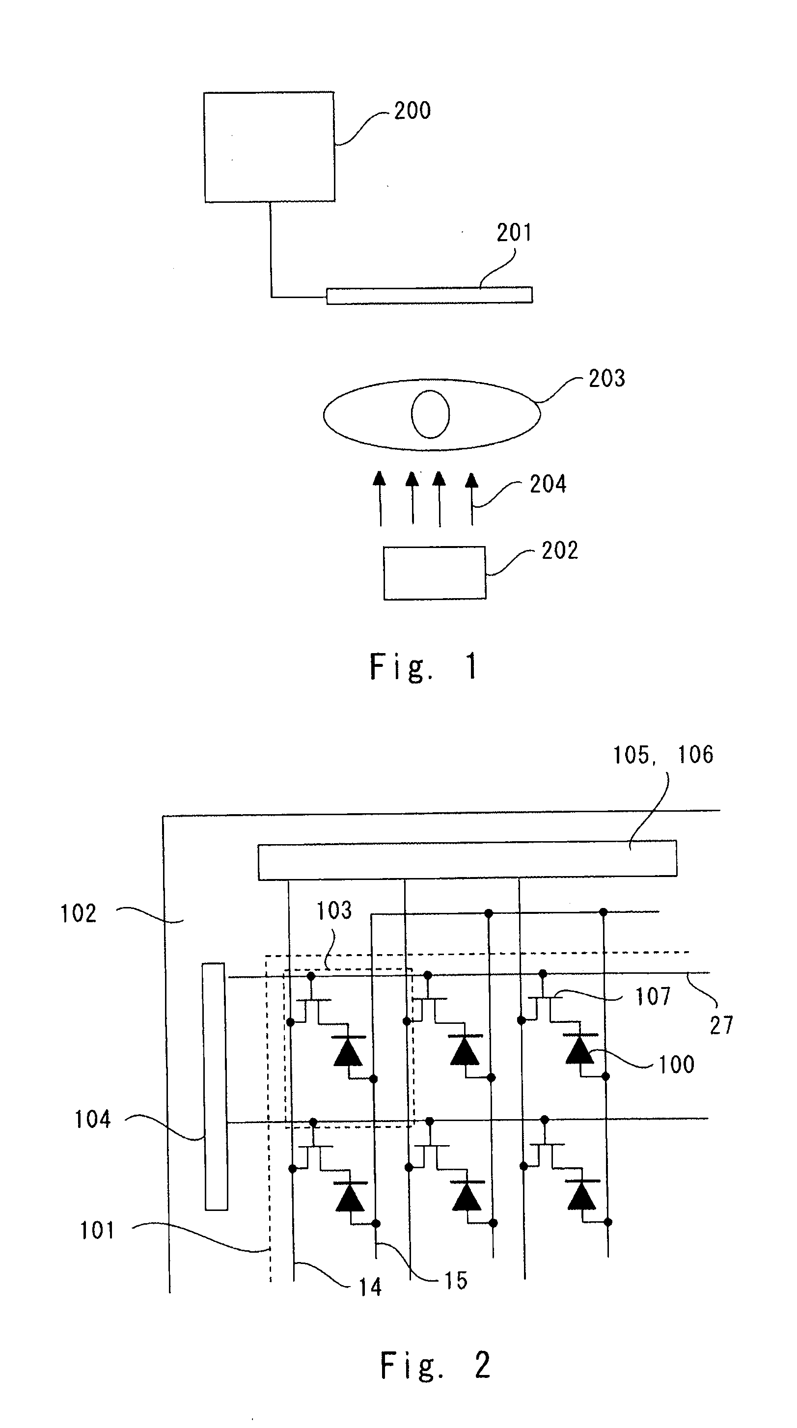
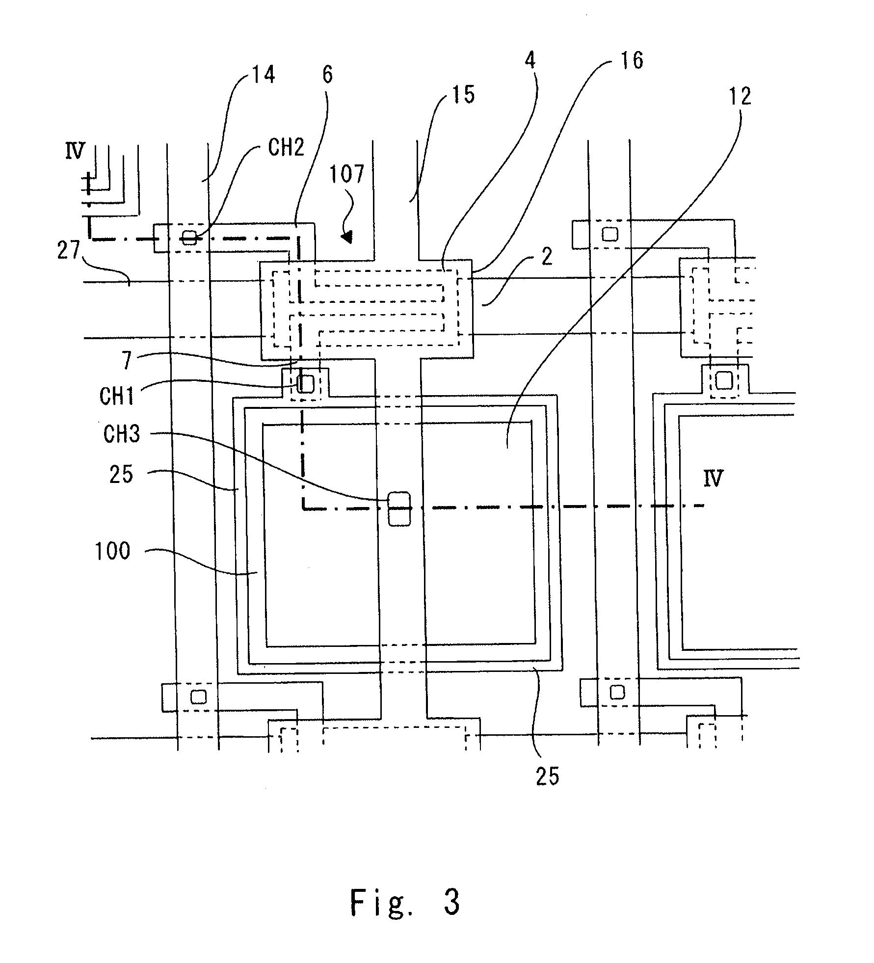
[0028]An exemplary embodiment of the present invention is described hereinafter with reference to the drawings. A photosensor according to the exemplary embodiment is used in an X-ray imaging device, for example. Referring first to FIG. 1, an X-ray imaging device is described. FIG. 1 is a schematic view showing a structure of an X-ray imaging device.
[0029]Referring to FIG. 1, an X-ray imaging device includes an image processing device 200, a photosensor 201 and an X-ray source 202. The photosensor 201, which is a flat panel, and the X-ray source 202 are placed opposite to each other. The photosensor 201 outputs a signal depending on the intensity of incident light. The photosensor 201 includes a scintillator that converts X rays into visible light. The photosensor 201 is connected to the image processing device 200. The image processing device 200 is an information processing device such as a personal computer. The image processing device 200 performs predetermined processing on out...
second exemplary embodiment
[0111]Another exemplary embodiment of the present invention is described hereinafter with reference to the drawings. In this exemplary embodiment, a high concentration oxygen-containing conductive layer 12a is provided in place of the nitrogen-containing semiconductor layer 11a as an anti-diffusion layer. The other structure, manufacturing method or the like is the same as those of the first exemplary embodiment, and description is thus omitted or simplified as appropriate. FIG. 10 is a sectional view showing a structure of a TFT substrate included in a photosensor according to the exemplary embodiment. FIG. 10 is a sectional view along line IV-IV in FIG. 3. Thus, FIG. 10 is a sectional view in the same part as FIG. 4.
[0112]The structure of the layers below the lower electrode 25 of the photodiode 100 is the same as that of the first exemplary embodiment, and description thereof is omitted. In the upper layer of the lower electrode 25, the photodiode 100 having a three-layer structu...
third exemplary embodiment
[0121]Another exemplary embodiment of the present invention is described hereinafter with reference to the drawings. In this exemplary embodiment, a silicide layer 20 is provided as an anti-diffusion layer in place of the nitrogen-containing semiconductor layer 11a. The other structure, manufacturing method or the like is the same as those of the first exemplary embodiment, and description is thus omitted or simplified as appropriate. FIG. 11 is a sectional view showing a structure of a TFT substrate included in a photosensor according to the exemplary embodiment. FIG. 11 is a sectional view along line IV-IV in FIG. 3. Thus, FIG. 11 is a sectional view in the same part as FIG. 4.
[0122]The structure of the layers below the lower electrode 25 of the photodiode 100 is the same as that of the first exemplary embodiment, and description thereof is omitted. In the upper layer of the lower electrode 25, the photodiode 100 having a three-layer structure in which the n-type semiconductor lay...
PUM
 Abstract
Description
Claims
Application Information
 - R&D
- Intellectual Property
- Life Sciences
- Materials
- Tech Scout
- Unparalleled Data Quality
- Higher Quality Content
- 60% Fewer Hallucinations
Browse by: Latest US Patents, China's latest patents, Technical Efficacy Thesaurus, Application Domain, Technology Topic, Popular Technical Reports.
© 2025 PatSnap. All rights reserved.Legal|Privacy policy|Modern Slavery Act Transparency Statement|Sitemap|About US| Contact US: help@patsnap.com