MSD integrated circuits with shallow trench

a technology of integrated circuits and trenches, which is applied in the direction of semiconductor devices, semiconductor/solid-state device details, diodes, etc., can solve the problems of high gate charge, poor performance, and high manufacturing cost of conventional deep gate trenches, so as to reduce the space occupied and improve the effect of performan

Inactive Publication Date: 2010-09-23
FORCE MOS TECH CO LTD
View PDF5 Cites 39 Cited by
  • Summary
  • Abstract
  • Description
  • Claims
  • Application Information

AI Technical Summary

Benefits of technology

[0005]It is therefore an aspect of the present invention to provide improved semiconductor power device configuration and manufacture processes for providing trench MOSFET dev...

Problems solved by technology

However, assembly of those separately structures into single package with extra interconnection wires results in higher manufacturing cost, and poor performance due to increase in inductance from the extra interconnection wires.
Another constraint is that, whe...

Method used


Image

  • MSD integrated circuits with shallow trench
  • MSD integrated circuits with shallow trench
  • MSD integrated circuits with shallow trench

Examples


first embodiment

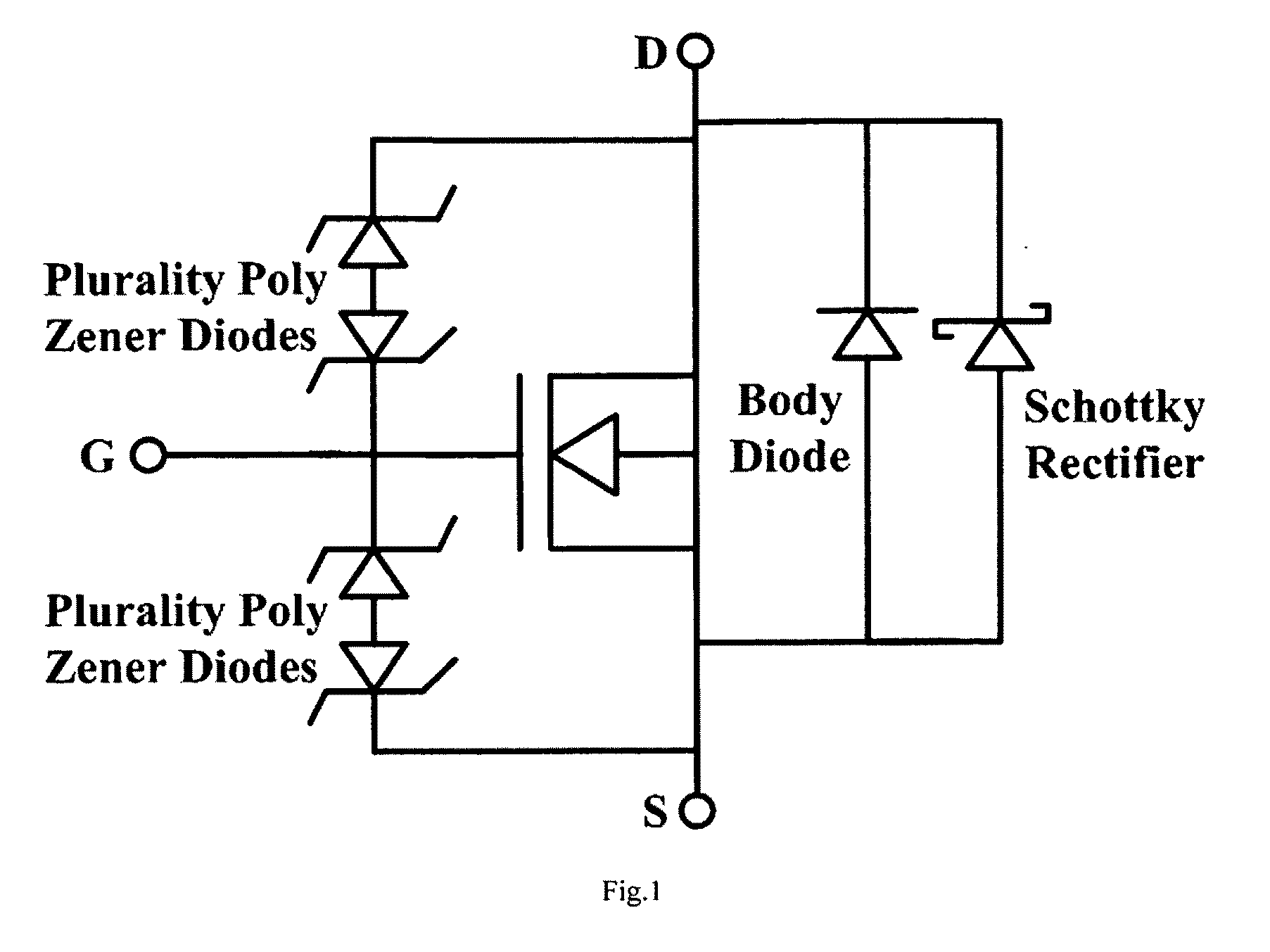
[0027]FIG. 5B is another cross-section C-D of the first embodiment as shown in FIG. 5C. The only difference between FIG. 5B and FIG. 5A is that there is an open area 250 of the drain metal on the top of the termination. A conventional metal field plate in the termination is provided to sustain breakdown voltage.

[0028]FIG. 5C is a top view of the first embodiment which shows Gate-Drain diode across termination with the open areas 250 in FIG. 5B of the drain metal. These open areas allow electrical field penetrate through the oxides during avalanche, and thus make benefits to avoid avalanche degradation caused by the metal field plate cross over the termination as shown in FIG. 5A.

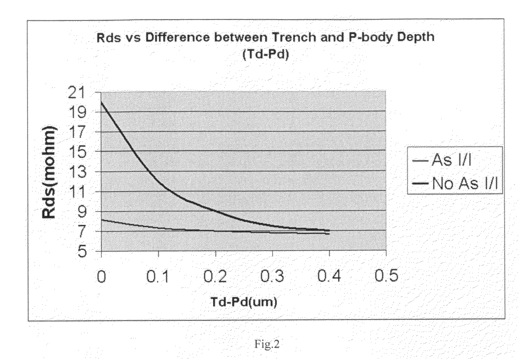
[0029]FIG. 6 is a normalized measurement result of the relationship between breakdown voltage and metal width cross over metal field plate termination, which shows that breakdown voltage will be degraded when metal width W is greater than 5 um, It means that electrical field underneath the cross-over metal c...

second embodiment

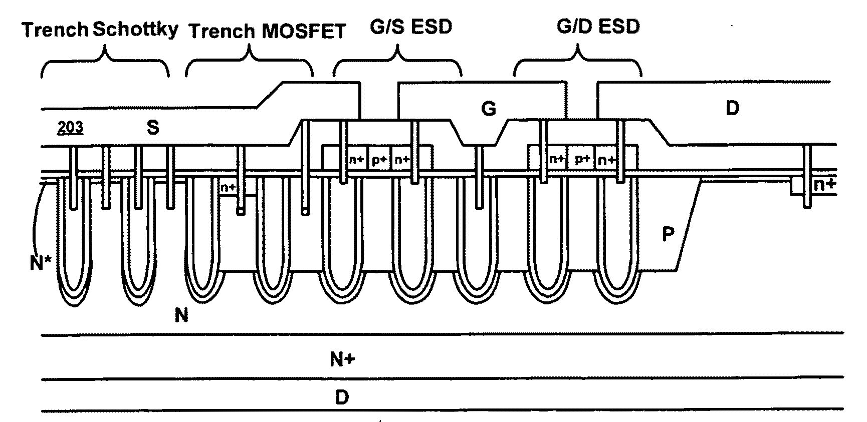
[0030]FIG. 7A is the cross-section A-B of the present invention. The only difference between the structure of FIG. 7A and FIG. 5.A is that the embedded Schottky rectifier is a trench Schottky rectifier instead of junction barrier Schottky rectifier. The trench Schottky contact trench 272 is formed in said N epitaxial layer and other contact trench 271 formed in the trench gate 270 adjacent to said contact trench.

[0031]FIG. 7B is another cross-section C-D of the second embodiment. The only difference between FIG. 7B and FIG. 7A is that there is an open area 251 of the drain metal on the top of the termination.

[0032]FIGS. 8A to 8D is a serial of exemplary steps that are performed to form the inventive device configuration of FIG. 7A. FIG. 8A shows that an N doped epitaxial layer 200 is grown on an N+ doped substrate 201. A trench mask (not shown) is applied to open a plurality of trenches by employing a dry silicon etch process. In order to remove the plasma damage introduced in etchi...


PUM


Abstract

A trench MOSFET device with embedded Schottky rectifier, gate-drain and gate-source diodes on single chip is formed with shallow trench structure to achieve device shrinkage and performance improvement. The present semiconductor devices achieve low Vf and reverse leakage current for embedded Schottky rectifier, have overvoltage protection for GS clamp diodes and avalanche protection for GD clamp diodes. More particularly, gate charge of the present semiconductor device is reduced due to the shallow trench surrounded by an additional N doped area around the bottom while keeping Rds low enough and at the same time, maintaining BV at a certain level

Description

FIELD OF THE INVENTION [0001]This invention relates generally to the cell structure, device configuration and fabrication process of power semiconductor devices. More particularly, this invention relates to an improved cell configuration and processes to manufacture trench MOSFET device with Schottky rectifier, Gate-Drain (GD) and Gate-Source (GS) diodes with shallow trench structure on single chip for device shrinkage and performance improvement.BACKGROUND OF THE INVENTION[0002]As shown in FIG. 1, normally for high efficiency DC / DC application, a Schottky rectifier is externally added in parallel with a MOSFET device to prevent a parasitic P / N body diode in the MOSFET from turning on in order to achieve higher speed and efficiency. The requirement for the clamping effect is that the forward voltage of the Schottky rectifier Vf is less than the parasitic body PN diode (˜0.7V). Besides the Schottky rectifier, a Gate-Source clamp diode with a breakdown voltage lower than the gate oxid...

Claims


Application Information

Patent Timeline
IPC IPC(8): H01L27/06
CPCH01L29/0619H01L29/8725H01L29/0878H01L29/1095H01L29/402H01L29/407H01L29/41766H01L29/4236H01L29/66727H01L29/66734H01L29/7806H01L29/7808H01L29/7811H01L29/7813H01L29/872H01L29/0638
Inventor HSIEH, FU-YUAN
Owner FORCE MOS TECH CO LTD
Why Eureka
Try Eureka