Transparent nonvolatile memory thin film transistor and method of manufacturing the same

a thin film transistor and non-volatile technology, applied in the direction of thermoelectric device junction materials, semiconductor devices, electrical equipment, etc., can solve the problems of affecting affecting the quality of oxide resistive memory, and affecting the quality of the entire electronic system, so as to reduce the process temperature and ensure the effect of process compatibility

Active Publication Date: 2010-09-30
ELECTRONICS & TELECOMM RES INST
View PDF2 Cites 37 Cited by
  • Summary
  • Abstract
  • Description
  • Claims
  • Application Information

AI Technical Summary

Benefits of technology

[0021]The present invention is directed to a structure of a transparent nonvolatile memory thin film transistor (TFT) applicable to the field of transparent electronic systems and a method of manufacturing the memory TFT. The transparent nonvolatile memory TFT according to the present invention may employ an organic ferroelectric thin layer and an oxide semiconductor thin layer, reduce a process temperature, and ensure process compatibility.
[0022]Also, the present invention is directed to a stack structure of a gate insulating layer of a transparent nonvolatile memory TFT applicable to a transparent electronic system, which may reduce an operating voltage and improve operating reliability, and a method of manufacturing the gate insulating layer.

Problems solved by technology

First, there is a growing tendency for electronic devices and systems to be formed on flexible substrates, abandoning the conventional silicon-based electronic devices that are hard and breakable.
First, the memory device should be nonvolatile. In general, memory devices may be divided into volatile memories and nonvolatile memories. A volatile memory stores data only when power is supplied, while a nonvolatile memory may retain data even when power is interrupted. Since the transparent electronic system is highly likely to be a stand-alone electronic device to which power is always supplied or a design-oriented application with a highlighted mobile function, a nonvolatile data storage function is required to increase the lifespan of a battery and store a large amount of data.
Second, an operating voltage of the memory should be within a predetermined range. When a memory operation requires an excessively high operating voltage through excessive emphasis on transparency, the entire electronic system may be adversely affected, and mounting the memory device in the electronic system or an integrated circuit (IC) becomes unnecessary. In addition, the memory device should ensure stable operations within the range of an operating voltage of a module used along with the memory device.
Third, the memory device should not be excessively large. A transparent memory device for a transparent electronic system would not only store data but also serve as an embedded memory device with additional functions. Accordingly, the memory device should be as small as possible so as not to excessively increase the size of the entire system.
Fourth, the memory device should ensure device stability suitable for operations required by the transparent electronic system. A typical nonvolatile memory device should also satisfy some reliability items.
However, the principle that the resistance of a material forming the oxide resistive memory device varies according to the intensity or direction of an applied voltage has not yet been closely examined, and it is known that the oxide resistive memory undergoes big differences in characteristics when materials of upper and lower electrodes are varied.
In other words, it is difficult to ensure characteristic uniformity of the oxide resistive memory, and the operating principles of the oxide resistive memory are unclear.
Thus, the oxide resistive memory cannot be used as an embedded memory for a system.
However, since the nano-floating gate memory uses an oxide semiconductor thin layer, it is far more difficult to quantitatively control the storage of charges than in a case in which a silicon semiconductor layer is used.
Furthermore, the drive of an oxide semiconductor thin layer using an accumulation layer and a depletion layer precludes low-voltage operations.
Since an oxide-based ferroelectric thin layer is typically crystallized at a temperature of about 500° C. or higher, the crystallization is not compatible with a process of forming a transparent oxide semiconductor layer at a temperature of about 300° C. or lower.
In addition, when a ferroelectric thin layer is formed of an organic material, a large leakage current is generated and it is difficult to thin out the ferroelectric thin layer and apply the ferroelectric thin layer to memory devices.

Method used


Image

  • Transparent nonvolatile memory thin film transistor and method of manufacturing the same
  • Transparent nonvolatile memory thin film transistor and method of manufacturing the same
  • Transparent nonvolatile memory thin film transistor and method of manufacturing the same

Examples


Embodiment Construction

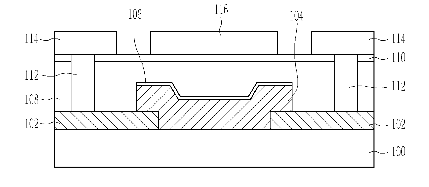
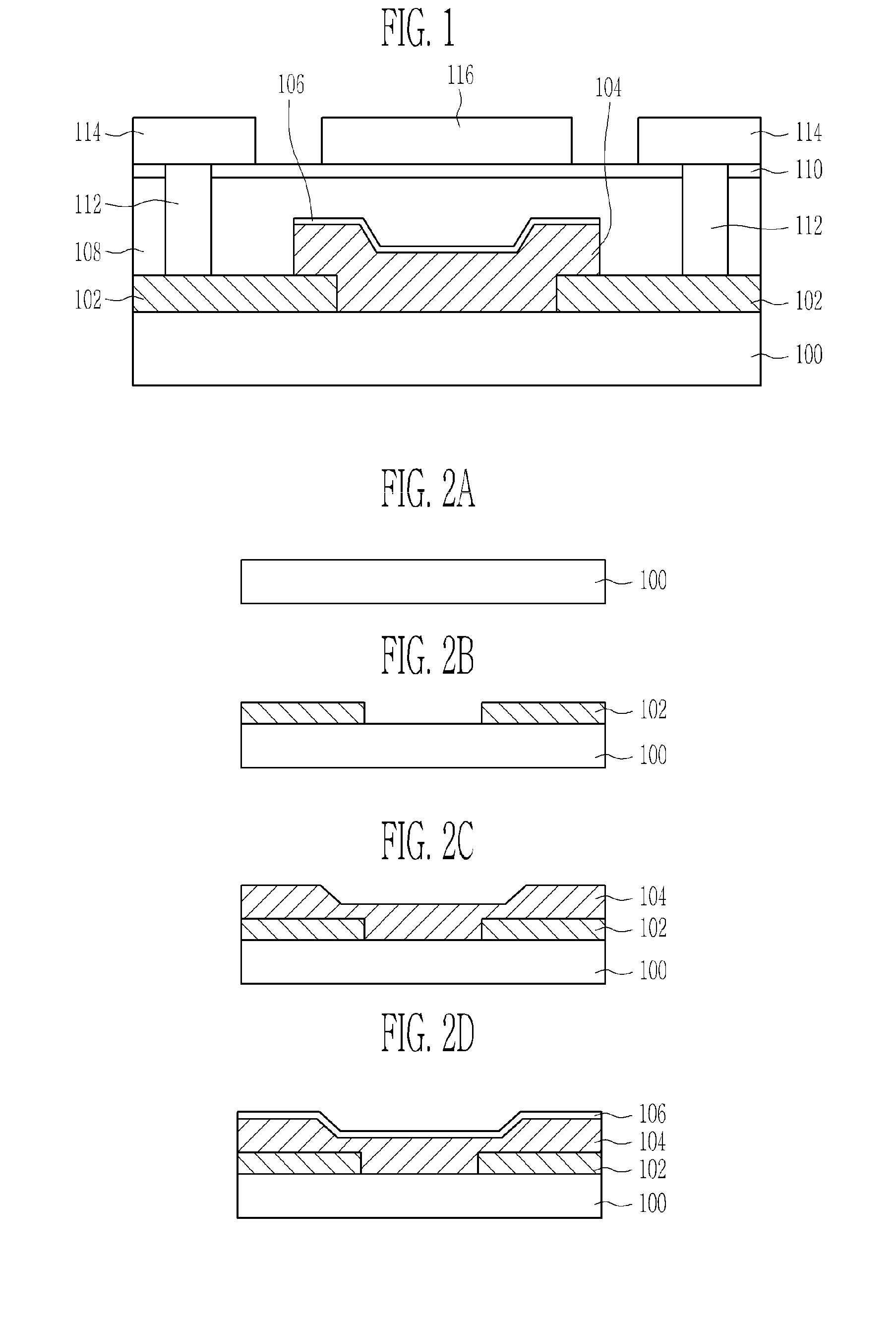
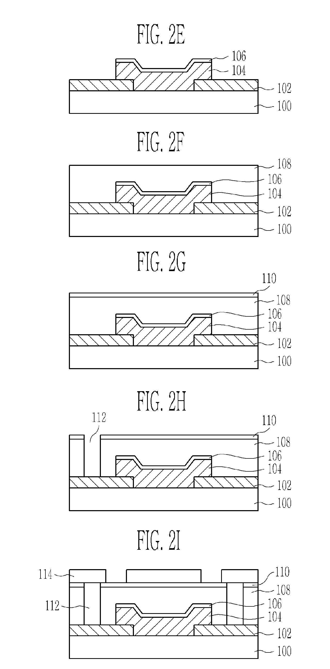
[0058]The present invention will be described more fully hereinafter with reference to the accompanying drawings, in which exemplary embodiments of the invention are shown. This invention may, however, be embodied in many different forms and should not be construed as being limited to the embodiments set forth herein. Rather, these embodiments are provided so that this disclosure is thorough and complete and fully conveys the concept of the invention to those skilled in the art. In the drawings, portions irrelevant to a description of the invention are omitted for brevity, and like numbers refer to like elements throughout.

[0059]It will be understood that the terms “comprises,”“comprising,”“has,”“having,”“includes,”“including” and / or variations thereof, when used in this specification, specify the presence of stated features, regions, steps, operations, elements, and / or components, but do not preclude the presence or addition of one or more other features, regions, steps, operations...


PUM


Abstract

Provided are a transparent nonvolatile memory thin film transistor (TFT) and a method of manufacturing the same. The memory TFT includes source and drain electrodes disposed on a transparent substrate. A transparent semiconductor thin layer is disposed on the source and drain electrodes and the transparent substrate interposed between the source and drain electrodes. An organic ferroelectric thin layer is disposed on the transparent semiconductor thin layer. A gate electrode is disposed on the organic ferroelectric thin layer in alignment with the transparent semiconductor thin layer. Thus, the transparent nonvolatile memory TFT employs the organic ferroelectric thin layer, the oxide semiconductor thin layer, and auxiliary insulating layers disposed above and below the organic ferroelectric thin layer, thereby enabling low-cost manufacture of a transparent nonvolatile memory device capable of a low-temperature process.

Description

CROSS-REFERENCE TO RELATED APPLICATION[0001]This application claims priority to and the benefit of Korean Patent Application No. 10-2009-0026068, filed Mar. 26, 2009, the disclosure of which is incorporated herein by reference in its entirety.BACKGROUND[0002]1. Field of the Invention[0003]The present invention relates to a transparent nonvolatile memory thin film transistor (TFT), and more specifically, to a transparent nonvolatile memory TFT in which the physical properties and materials of respective components of a gate stack of the TFT are optimized to allow the TFT to be transparent in a visible light region, undergo a low-temperature process, and perform low-voltage and high-speed operations, and a method of manufacturing the TFT.[0004]2. Discussion of Related Art[0005]The electronics industry has been developing so far through the advancement of silicon-based materials and device technology. Electronic components of the electronics industry are composed of a large number of s...

Claims


Application Information

Patent Timeline
Patent Type & Authority Applications(United States)
IPC IPC(8): H01L27/115H01L51/10H01L29/12H01L21/8246
CPCH01L21/28291H01L29/78391H01L29/7869H01L29/40111H01L29/6684
Inventor YOON, SUNG MINYANG, SHIN HYUKJUNG, SOON WOONKANG, SEUNG YOULCHO, DOO HEEBYUN, CHUN WONHWANG, CHI SUNYU, BYOUNG GONCHO, KYOUNG IK
Owner ELECTRONICS & TELECOMM RES INST
Why Eureka
Try Eureka