Wiring board and method of manufacturing the same
a wiring board and manufacturing method technology, applied in the direction of printed circuit aspects, conductive pattern formation, semiconductor/solid-state device details, etc., can solve the problems of low fluidity of resin, crack generation in resin, and inability to effectively suppress the generation of voids, so as to achieve sufficient bonding strength, the effect of increasing the fluidity of the underfill resin and increasing the fluidity
- Summary
- Abstract
- Description
- Claims
- Application Information
AI Technical Summary
Benefits of technology
Problems solved by technology
Method used
Image

Examples
first embodiment
See FIGS. 1a to 5d
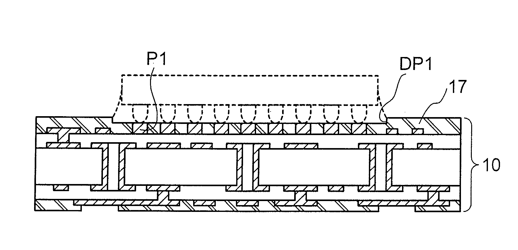
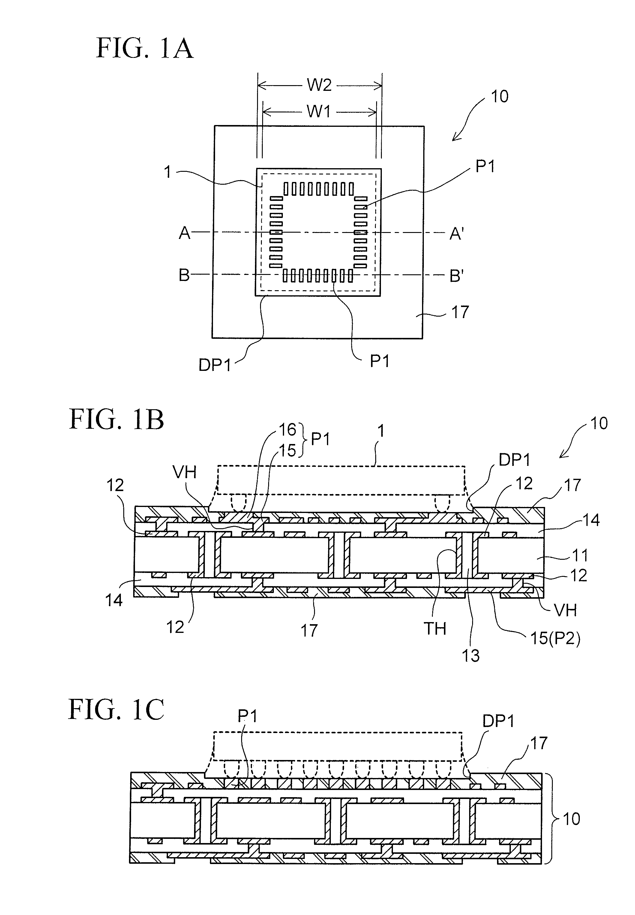
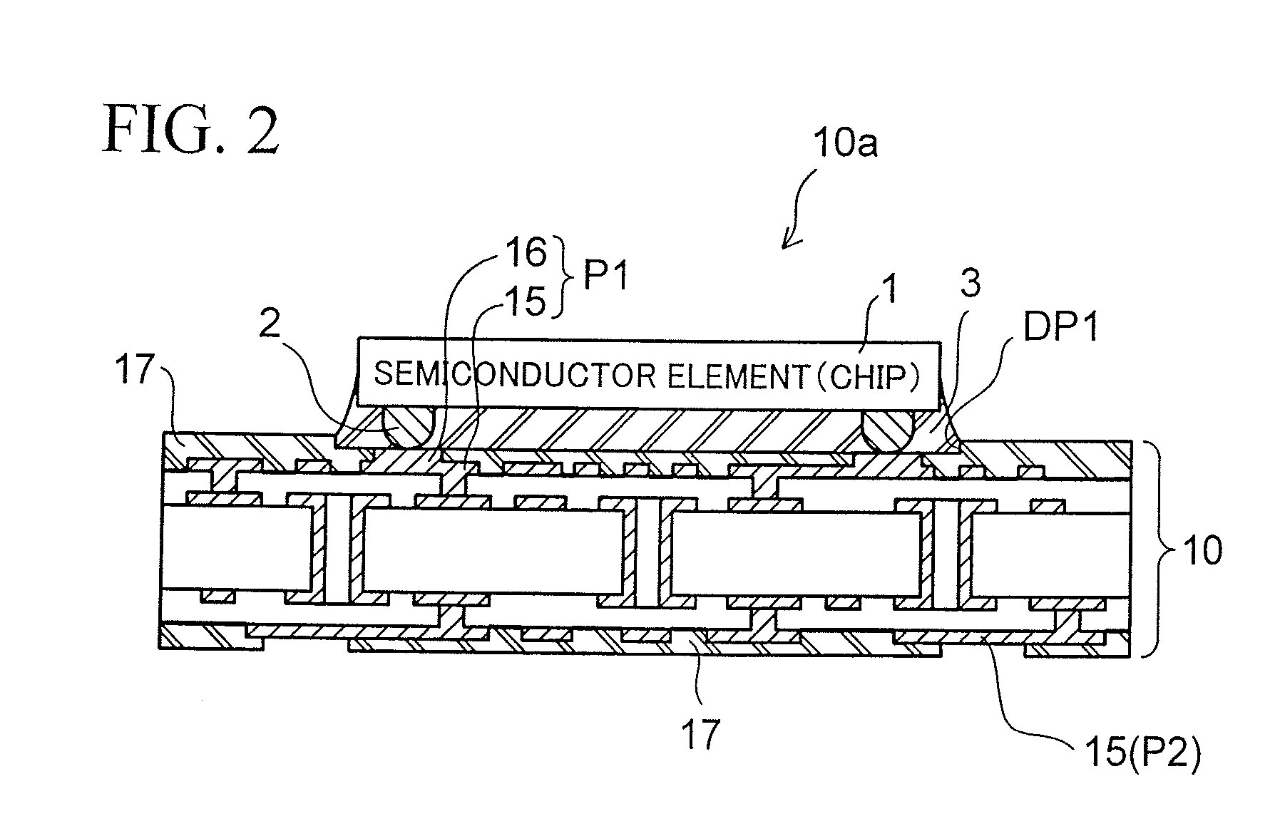
[0041]FIGS. 1A to 1C show a configuration of a wiring board (semiconductor package) according to a first embodiment of the present invention. FIG. 1A shows the wiring board as viewed from above. FIG. 1B shows the wiring board as viewed in a vertical cross-sectional view taken along the line A-A′ of FIG. 1A. FIG. 10 shows the wiring board when viewed in a vertical cross-sectional view taken along the line B-B′ of FIG. 1A.
[0042]A wiring board (semiconductor package) 10 according to the first embodiment is for use in flip-chip mounting of a semiconductor integrated circuit device (semiconductor chip 1 illustrated by a broken line) having a peripheral type terminal arrangement as illustrated.
[0043]The wiring board 10 of the present embodiment is basically configured to have a multi-layer wiring board fabricated by using a general build-up method. In the illustrated example, wiring layers (wiring patterns) 12 are formed on both surfaces of a core substrate 11 serving a...
second embodiment
See FIGS. 6a to 9d
[0085]FIGS. 6A and 6B are diagrams for showing a configuration of a wiring board (semiconductor package) according to a second embodiment of the present invention. FIG. 6A shows the configuration when the wiring board is viewed from above, and FIG. 6B shows the configuration when the wiring board is viewed in a cross section taken along the like A-A′ of FIG. 6A, likewise.
[0086]As compared with the configuration of the wiring board 10 according to the first embodiment (FIGS. 1A to 1C), a wiring board (semiconductor package) 20 according to the second embodiment is different in that pads P3 for flip-chip bonding (shape of each of the pads P3 is a “circle”) are arranged in a matrix so as to match the terminal arrangement (matrix type) of a semiconductor chip 1a to be mounted thereon. The other configuration of the wiring board 20 is basically the same as the configuration of the wiring board 10 according to the first embodiment.
[0087]Namely, the wiring board 20 accor...
third embodiment
See FIGS. 10a to 14c
[0102]FIGS. 10A to 10C are diagrams provided for showing a configuration of a wiring board (semiconductor package) according to a third embodiment of the present invention. FIG. 10A shows the configuration when the wiring board is viewed from above, FIG. 10B shows the configuration when the wiring board is viewed in a cross section taken along the line A-A′ of FIG. 10A, and FIG. 10C shows the configuration when the wiring board is viewed in a vertical cross section taken along the like B-B′ of FIG. 10A, likewise.
[0103]As compared with the configuration of the wiring board 10 (FIGS. 1A to 1C), a wiring board (semiconductor package) 30 according to the third embodiment is different in that a wiring layer 35 positioned outermost on the chip mounting surface side is formed into a step-like shape (in the form of three-dimensional wiring), that pads P5 for flip-chip bonding are defined at portions on the wiring layers 35 in the step-like shape, and that portions (conv...
PUM
| Property | Measurement | Unit |
|---|---|---|
| temperature | aaaaa | aaaaa |
| thickness | aaaaa | aaaaa |
| thickness | aaaaa | aaaaa |
Abstract
Description
Claims
Application Information
 - R&D
- Intellectual Property
- Life Sciences
- Materials
- Tech Scout
- Unparalleled Data Quality
- Higher Quality Content
- 60% Fewer Hallucinations
Browse by: Latest US Patents, China's latest patents, Technical Efficacy Thesaurus, Application Domain, Technology Topic, Popular Technical Reports.
© 2025 PatSnap. All rights reserved.Legal|Privacy policy|Modern Slavery Act Transparency Statement|Sitemap|About US| Contact US: help@patsnap.com