[0014]The present invention provides an improved design for an epitaxial reactor with higher
throughput, a wafer sleeve containing a multiplicity of wafers within a small reaction volume to improve usage of process gases and minimize unwanted deposition on the
reaction chamber walls, and increased lamp lifetimes through improved lamp
temperature control. A high degree of control over film thickness and resistivity uniformities within and between wafers may be achieved in the present invention without the need for rotary or other types of wafer motion during the
deposition process, thereby simplifying the design of the reactor chamber. The epitaxial reactor of the present invention may comprise one or more lamp modules which irradiate a wafer sleeve contained within a reactor frame which also supports the lamp modules. Alternative embodiments of the present invention may employ either resistive heating or inductive heating of the wafer sleeve, instead of radiant lamp heating.
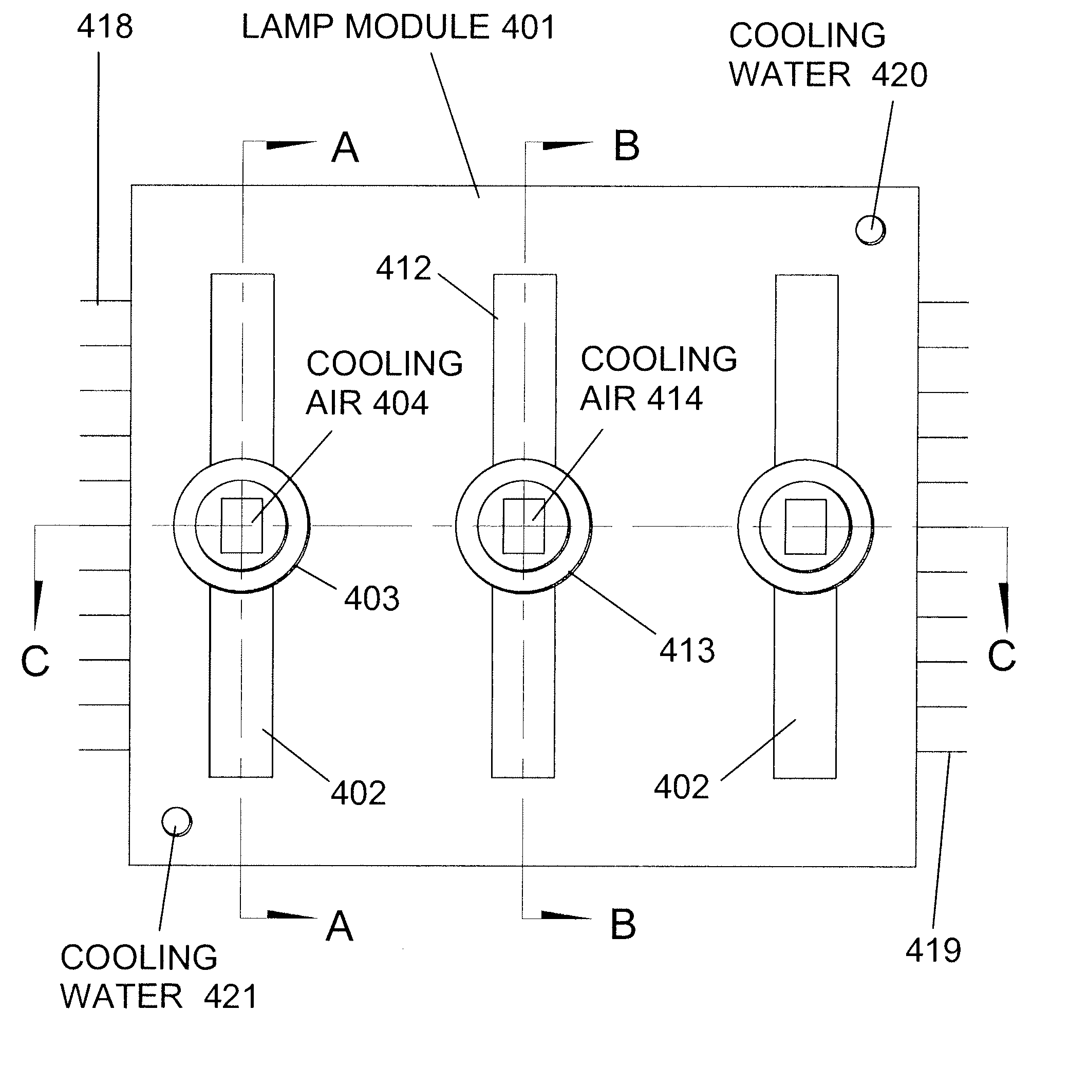
[0017]The process gases for epitaxial deposition may be fed directly into the
interior space of the wafer sleeve by a set of process gas inlet tubes on the top and bottom of the reactor frame. Also on the top of the reactor frame is a set of purge gas inlet tubes, typically supplying
hydrogen gas into the volume within the reactor frame, but outside of the wafer sleeve. Thus, a minimum amount of purge gas is introduced into the outer portions of the reactor module, thereby minimizing the amount of undesirable deposition on surfaces outside of the interior of the reactor module. Deposition on the inner surfaces of the reactor module is further reduced by
water cooling of the reactor module. A set of exhaust outlet lines extends out of the top and bottom of the reactor frame. The exhaust gases comprise the purge gas, products from the epitaxial reaction within the reactor module, and unused reactant gases.
[0020]In a first embodiment of the overall
system of the present invention, the epitaxial reactor may be integrated within a
system comprising a preheat chamber, a single epitaxial deposition reactor, and a cool down chamber. In a second embodiment, two or more epitaxial deposition reactors may be employed in series, and combined with a preheat chamber and a cool down chamber. In this second embodiment, the epitaxial reactors each deposit part of the desired final film thickness. For example, in a system comprising a preheat chamber, three epitaxial reactors, and a cool down chamber, each of the epitaxial reactors could deposit approximately one third of the final desired film thickness. During deposition within each of the three epitaxial reactors, the cross-flow
deposition process could be employed to enhance deposition uniformity. Thus, the deposition time per epitaxial reactor would be one third that required for the single epitaxial reactor in the first embodiment. Assuming that the preheat and cool down times are less than one third of the total deposition time, this second embodiment could provide a wafer throughput roughly three times higher than the throughput of the first embodiment.
[0021]In a further embodiment of the present invention, a number of epitaxial reactors may be employed in series, with differing flow directions to achieve the desired overall film uniformity without the need for cross-flow
processing within any of the epitaxial reactors. This approach, which may be combined with a preheat chamber and a cool down chamber, enables simpler reactor chambers to be employed since each reactor would need
piping for only unidirectional process gas and exhaust flows.
[0022]Since the wafer sleeve of the present invention is heated by an array of lamps, a method of lamp sequencing may be employed to further enhance film deposition uniformities. In this method, the variation in
deposition rate along a direction corresponding to the process gas flows may be made nearly linear by activation of the heating lamps for various duty cycles less than 100%, thereby controlling the
deposition rate through real-
time control of the wafer temperatures in different parts of the wafer sleeves. Combining lamp sequencing with cross-flow processing could then enable relatively uniform overall deposition rates to be obtained within and between wafers.

