
Semiconductor memory device and method for manufacturing the same

a semiconductor memory and semiconductor technology, applied in the direction of semiconductor memory devices, electrical appliances, transistors, etc., can solve the problems of reducing the operational stability of the semiconductor memory device, increasing the amount of power consumption, and deteriorating the data transfer rate, so as to reduce parasitic capacitance and increase the operational stability

Active Publication Date: 2010-10-28
SK HYNIX INC
View PDF1 Cites 24 Cited by
  • Summary
  • Abstract
  • Description
  • Claims
  • Application Information

AI Technical Summary

Benefits of technology

The present invention provides a semiconductor memory device and a method for manufacturing the same that address issues related to limitations and disadvantages of the related art. The invention provides a semiconductor memory device with a cell region having a high operational stability by reducing parasitic capacitance. The method includes forming a buried word line in the cell region, depositing an insulation layer in the cell region and the peripheral region, and etching the insulation layer to form a bit line contact hole exposing the active region adjacent to the buried word line. The method also includes depositing a first conductive layer over the cell region and the peripheral region to form a bit line layer and an upper electrode layer. The invention also includes a semiconductor memory device with a bit line layer and an upper electrode layer, and a metal barrier layer between the bit line layer and the insulation layer and between the upper electrode layer and the lower electrode layer of the gate pattern. The invention further includes a storage node contact connected to the active region, and a channel region formed at a lower part of the buried word line in the cell region and has a three-dimensional structure in vertical and horizontal directions.

Problems solved by technology

The increase in resistance deteriorates a data transfer rate, increases the amount of power consumption, and finally results in a reduction in operational stability of the semiconductor memory device.
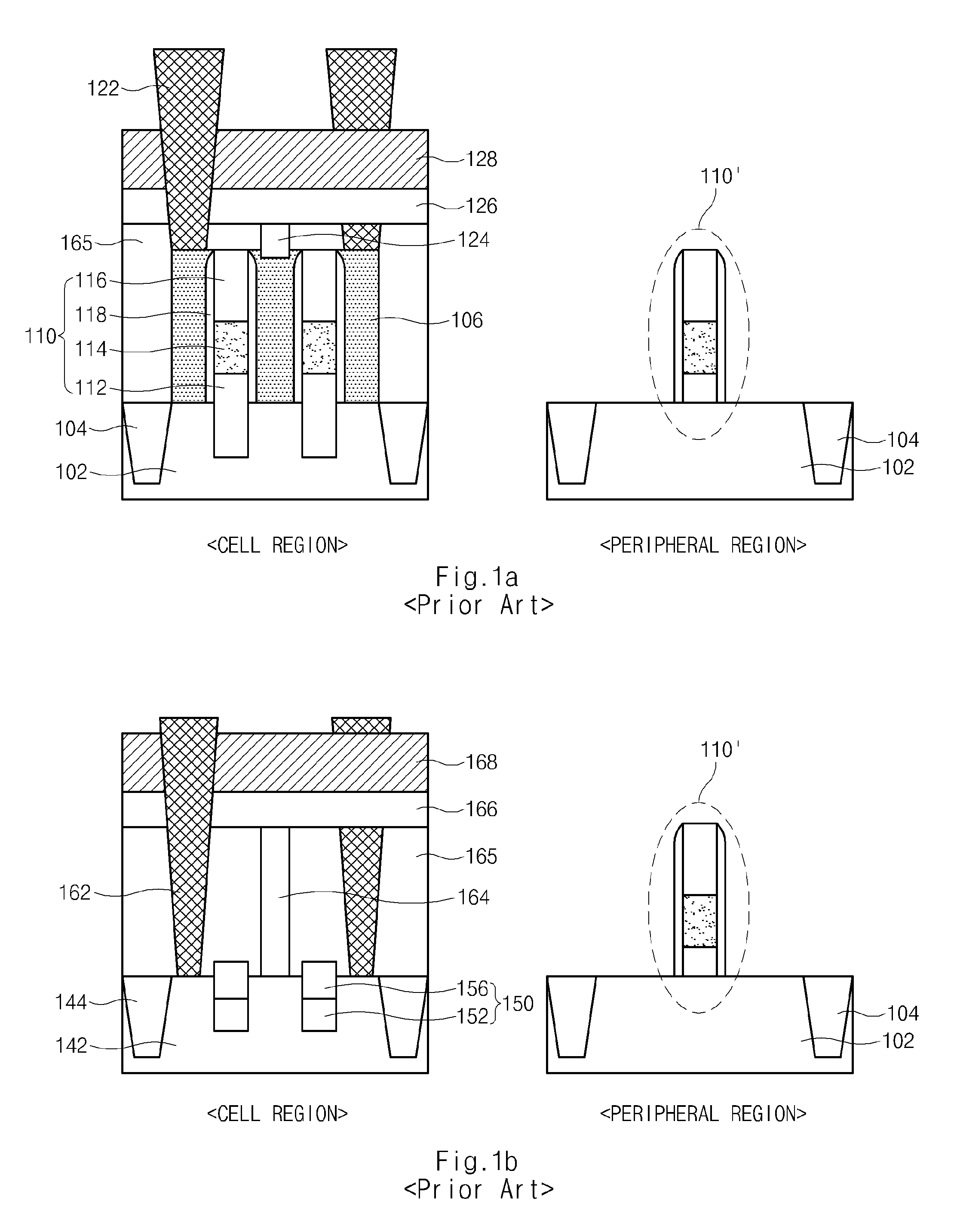
On the other hand, if the cross-sectional size of a word line or bit line is maintained as in the related art, when the degree of integration increases, a physical distance between a word line and a bit line is unavoidably reduced.
The bit line, used for transferring data received from a unit cell capacitor, may not operate normally due to the increase in parasitic capacitance and the high potential of the word line.
If data is not smoothly and normally transferred through the bit line, a sense amplifier used to detect and amplify data may not detect the data.
This results in a reading error.
However, the higher the degree of integration, the smaller the region occupied by the capacitor contained in the semiconductor memory device.
That is, there is a limitation in increasing the size of a capacitor contained in the unit cell while increasing the degree of integration of the semiconductor memory device.
The higher the degree of integration of the semiconductor memory device, the shorter a physical distance between neighboring conductive regions, resulting in the increase of parasitic capacitance.
However, it is difficult to expose the surface of an upper part of the active region 142 by etching the thickly-deposited insulation layer due to the reduction in the design rules.
This may cause a malfunction to occur in the semiconductor memory device.
In the meantime, a unit cell structure for restricting the occurrence of parasitic capacitance does not have a sufficient process margin for forming the storage node contact or the bit line contact plug, so that the possibility of generating an unexpected defective part in the unit cell structure increases.

Method used


Image

  • Semiconductor memory device and method for manufacturing the same
  • Semiconductor memory device and method for manufacturing the same
  • Semiconductor memory device and method for manufacturing the same

Examples


Embodiment Construction

[0042]Reference will now be made in detail to the embodiments of the present invention, examples of which are illustrated in the accompanying drawings. Wherever possible, the same reference numbers will be used throughout the drawings to refer to the same or like parts.

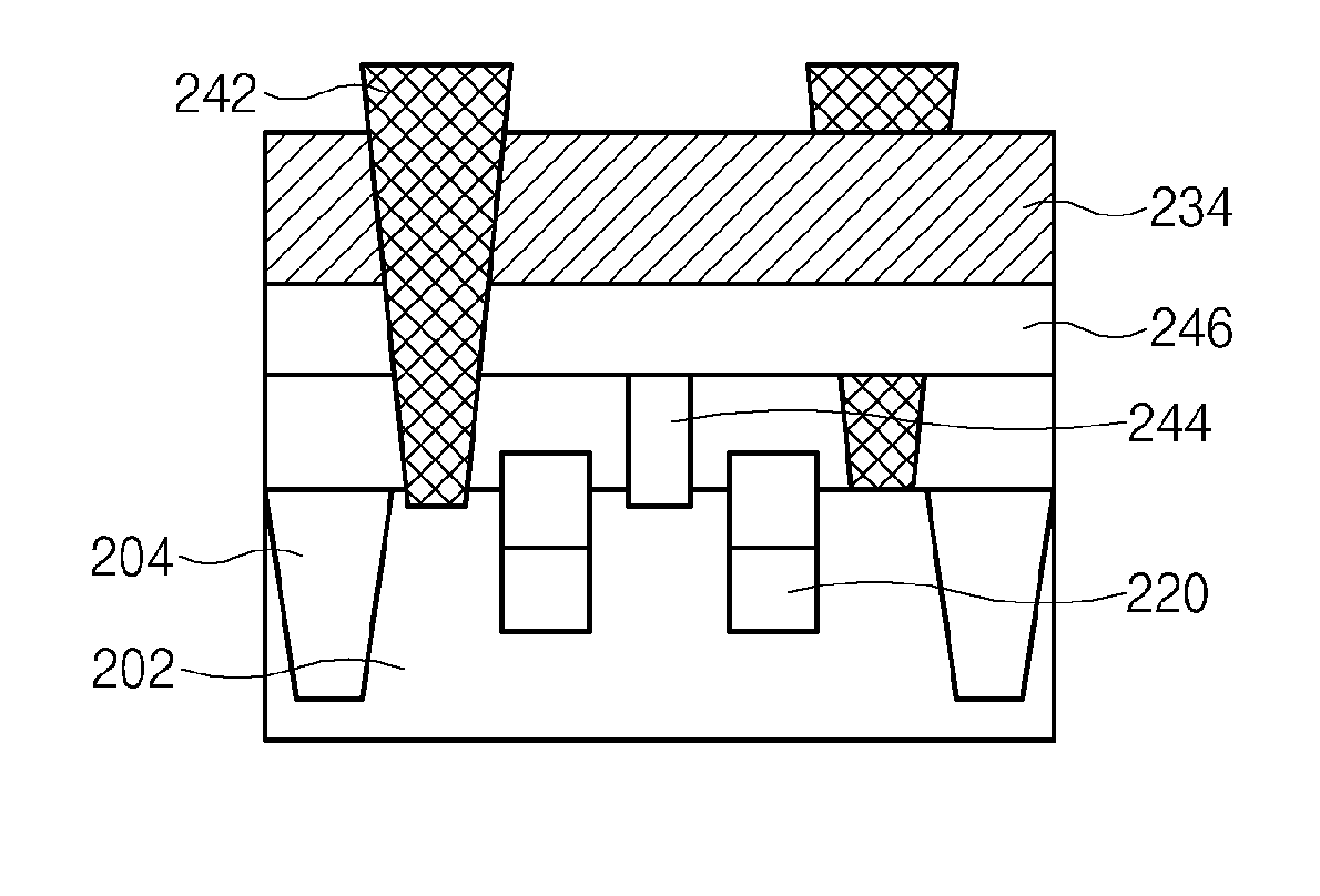
[0043]FIGS. 2a to 2o are cross-sectional views illustrating a semiconductor memory device and a method for manufacturing the same according to embodiments of the present invention.

[0044]Referring to FIG. 2a, through a shallow trench isolation insulating layer (STI) process, a device isolation layer (e.g., a STI layer) 204 for defining an active region 202 is formed in each of a cell region and peripheral region. The cell region is a region including a plurality of unit cells, and the peripheral region is a region including core and peripheral circuits (e.g., a power-supply circuit, a circuit for decoding commands and addresses, a local data line, and the like). Because a method for forming the device isolation layer 2...


PUM


Abstract

A semiconductor memory device and a method for manufacturing the same are disclosed, which reduce parasitic capacitance generated between a storage node contact and a bit line of a high-integration semiconductor device. A method for manufacturing a semiconductor memory device includes forming a buried word line in an active region of a cell region, forming an insulation layer in the cell region and a lower electrode layer of a gate in a peripheral region so that a height of the insulation layer is substantially equal to that of the lower electrode layer, and providing a first conductive layer over the cell region and the peripheral region to form a bit line layer and an upper electrode layer.

Description

CROSS-REFERENCE TO RELATED APPLICATION[0001]The priority of Korean patent application No. 10-2009-0036063 filed on Apr. 24, 2009, the disclosure of which is hereby incorporated in its entirety by reference, is claimed.BACKGROUND OF THE INVENTION[0002]The present invention relates to a semiconductor device, and more particularly to a semiconductor device and a method for manufacturing the same, which reduces parasitic capacitance of a bit line when forming a cell array contained in a high-integration semiconductor memory device.[0003]Semiconductor devices are formed by implanting impurities or depositing a new material at a predetermined region in a silicon wafer. A representative example of the semiconductor devices may be a semiconductor memory device. The semiconductor memory device includes a large number of elements, for example, transistors, capacitors, resistors, and the like. Individual elements are interconnected through a conductive layer so that data or signals are communi...

Claims


Application Information

Patent Timeline
Patent Type & Authority Applications(United States)
IPC IPC(8): H01L27/108H01L21/8242H10B12/00H10B99/00
CPCH01L21/823437H01L27/10873H01L27/1052H01L27/10891H01L27/10894H01L27/10876H10B12/05H10B12/053H10B12/488H10B12/09H01L21/02225H01L29/42312H10B12/482
Inventor CHOI, WOONG
Owner SK HYNIX INC
Learn More