Semiconductor image sensor module and method of manufacturing the same

a technology of image sensor and semiconductor, applied in the direction of semiconductor/solid-state device details, instruments, radiation control devices, etc., can solve the problems of inability to achieve simultaneous electronic shuttering, small area of a unit pixel, that is, a minute pixel, etc., to improve improve the utilization rate of the chip, and improve the effect of the aperture ratio of the photoelectric conversion elemen

Active Publication Date: 2010-11-04
SONY CORP
View PDF66 Cites 419 Cited by
  • Summary
  • Abstract
  • Description
  • Claims
  • Application Information

AI Technical Summary

Benefits of technology

[0025]According to a semiconductor image sensor module of the present invention, a first semiconductor chip provided with an image sensor in which a pixel is constituted by a photoelectric conversion element and transistors and a second semiconductor chip provided with an analog/digital converter array which is composed of a plurality of analog/digital converters are laminated to constitute the semiconductor image sensor module, so that in the first semiconductor chip, a large portion thereof can be formed as a pixel region and therefore, the aperture ratio of the photoelectric conversion element is improved and also, it is possible to improve chip utilization. Also, by providing a semiconductor chip which includes a memory element array composed of a plurality of memory elements, the pixel signals from the first semiconductor chip can be signal-processed after carrying out analog/digital conversion in the second semiconductor chip in a short period and once storing the signals in the memory element array, so that it is possible to realize simultaneous shuttering of the pixels.
[0026]By configuring a first semiconductor chip provided with an image sensor in which the pixel is constituted by a photoelectric conversion element and transistors, a second semiconductor chip provided with an analog/digital converter array which is composed of a plurality of analog/digital converters, and further a third semiconductor chip provided with a memory element array which includes at least a decoder and a sense amplifier, in a laminated structure, one unified device is obtained, and it is possible to realize improvement of the aperture ratio of the photoelectric conversion element, improvement of chip utilization, and further simultaneous shuttering o

Problems solved by technology

Owing to this fact, simultaneity of accumulation is not obtained, and simultaneous electronic shuttering cannot be obtained.
However, in the CMOS image sensor having the constitution of FIG. 52, the photodiode PD-sensor circuit region 32 and the ADC-memory region 33 are included in a single semiconductor chip

Method used


Image

  • Semiconductor image sensor module and method of manufacturing the same
  • Semiconductor image sensor module and method of manufacturing the same
  • Semiconductor image sensor module and method of manufacturing the same

Examples


Embodiment Construction

[0087]Hereinafter, exemplified embodiments of the present invention will be explained with reference to the drawings

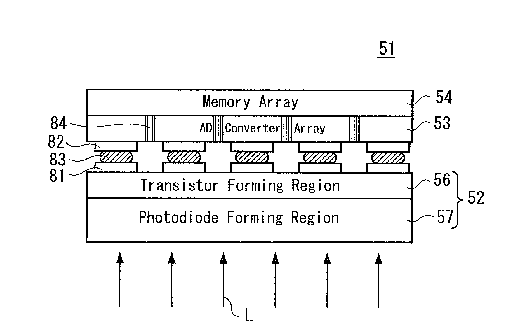
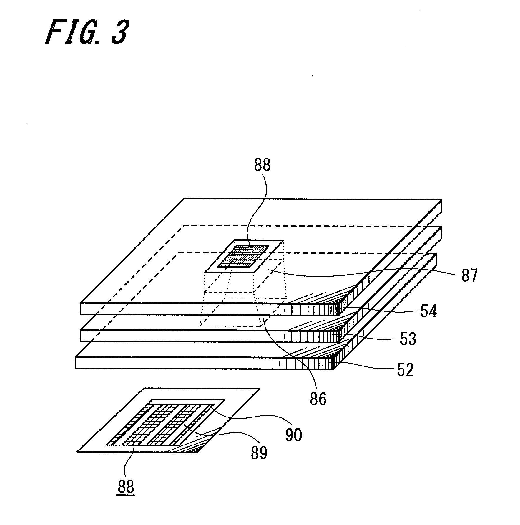
[0088]FIG. 1 shows a general constitution of a first exemplified embodiment of a semiconductor image sensor module according to the present invention. A semiconductor image sensor module 51 according to the exemplified embodiment of the present invention is constituted by laminating a first semiconductor chip 52 provided with an image sensor in which a plurality of pixels are arranged regularly and each of the pixels is constituted by a photodiode as a photoelectric conversion element and a transistor, a second semiconductor chip 53 provided with an analog / digital converter array composed of a plurality of analog / digital converters (a so-called analog / digital conversion circuit), and a third semiconductor chip 54 provided with a memory element array including at least a decoder and a sense amplifier.

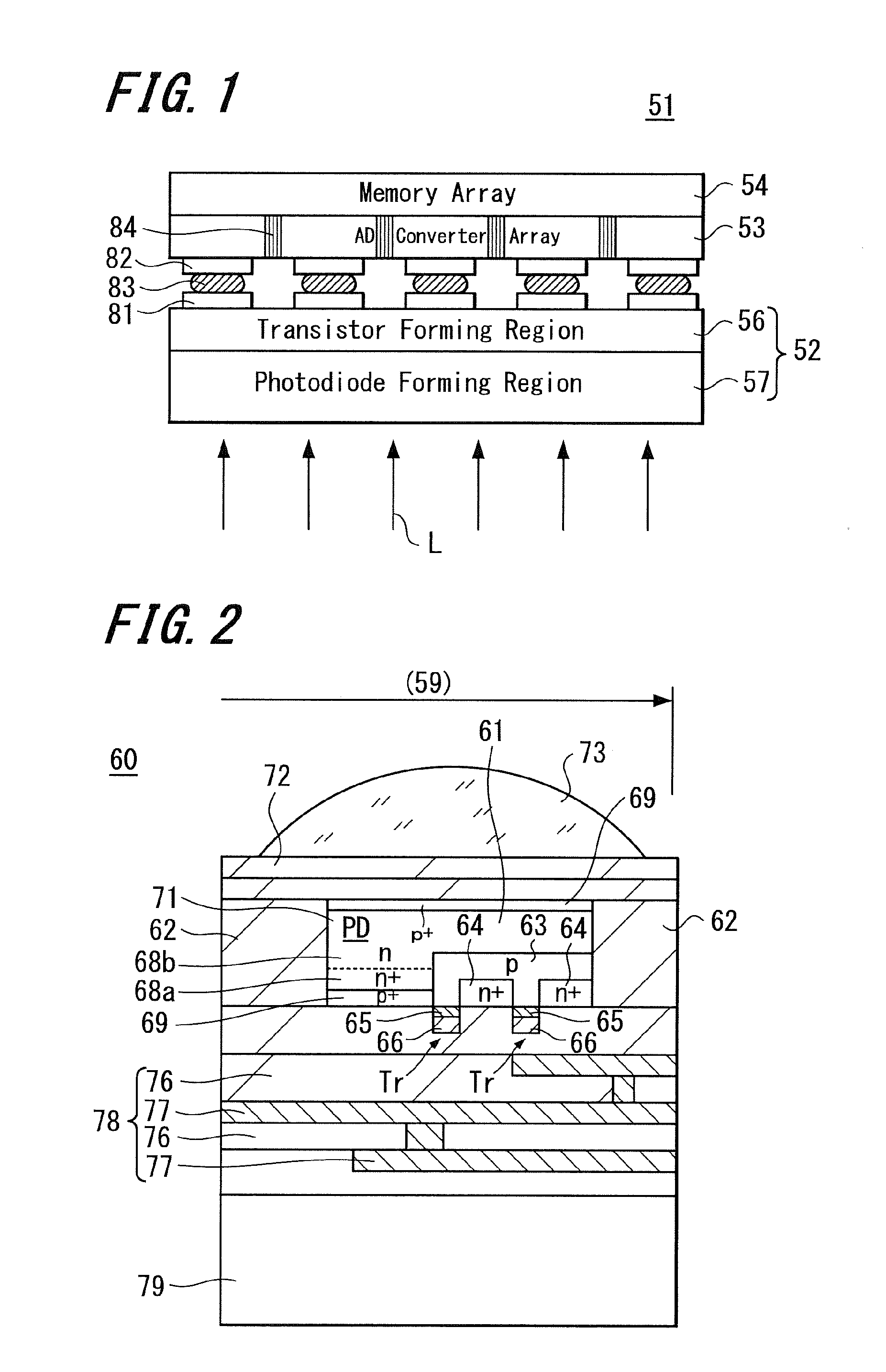
[0089]The image sensor of the first semiconductor chip 52 in this exam...


PUM


Abstract

A CMOS type semiconductor image sensor module wherein a pixel aperture ratio is improved, chip use efficiency is improved and furthermore, simultaneous shutter operation by all the pixels is made possible, and a method for manufacturing such semiconductor image sensor module are provided. The semiconductor image sensor module is provided by stacking a first semiconductor chip, which has an image sensor wherein a plurality of pixels composed of a photoelectric conversion element and a transistor are arranged, and a second semiconductor chip, which has an A/D converter array. Preferably, the semiconductor image sensor module is provided by stacking a third semiconductor chip having a memory element array. Furthermore, the semiconductor image sensor module is provided by stacking the first semiconductor chip having the image sensor and a fourth semiconductor chip having an analog nonvolatile memory array.

Description

TECHNICAL FIELD[0001]The present invention relates to a semiconductor image sensor module and a method of manufacturing the same. In more detail, it relates to a semiconductor image sensor module which realizes simultaneous shuttering meeting speeding up of the shutter speed of, for example, a digital still camera, a video camera, a mobile phone with a camera or the like.BACKGROUND ART[0002]Since a CMOS image sensor operates with a single power supply in low power consumption as compared with a CCD image sensor and can be manufactured by a standard CMOS process, there is an advantage that a system on chip is easy. In recent years, a CMOS image sensor has started to be used based on this advantage even in a high-grade single lens reflex type digital still camera and a mobile phone.[0003]In FIG. 54 and FIG. 55, simplified constitutions of a CCD image sensor and a CMOS image sensor are shown respectively.[0004]A CCD image sensor 1 shown in FIG. 54 is formed in a constitution that a plu...

Claims


Application Information

Patent Timeline
IPC IPC(8): H01L31/101H01L31/18H04N5/374H04N5/378
CPCH01L23/481H01L27/115H01L2924/0002H01L2924/00014H01L27/1464H01L2224/0401H01L2924/13091H01L27/14625H01L27/14627H01L27/14632H01L27/14634H01L27/1469H01L29/788H01L29/792H04N5/374H04N5/378H01L2224/0557H01L2224/13H01L2224/13025H01L2224/16145H01L2224/16237H01L27/14643H01L27/14689H01L2224/05554H01L2224/05552H01L2924/00H01L27/14612H01L27/14638H01L27/14607H01L27/14636H04N25/79H04N25/76H04N25/75H10B69/00H04N23/54H01L24/16H01L25/18H01L2924/1425H01L2924/1436H01L2924/1437H01L2924/1443
Inventor IWABUCHI, SHINMOTOYOSHI, MAKOTO
Owner SONY CORP
Why Eureka
Try Eureka