

Display device and method for production thereof
a technology of display panel and display panel, which is applied in the direction of luminescence, instrumentation, casing/cabinet/drawer of electrical apparatus, etc., can solve the problems of air layer, decrease in display contrast, and decrease in display panel transmissivity
- Summary
- Abstract
- Description
- Claims
- Application Information
AI Technical Summary
Benefits of technology
Problems solved by technology
Method used
Image

Examples
embodiment 1
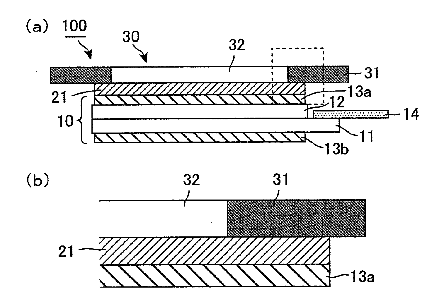
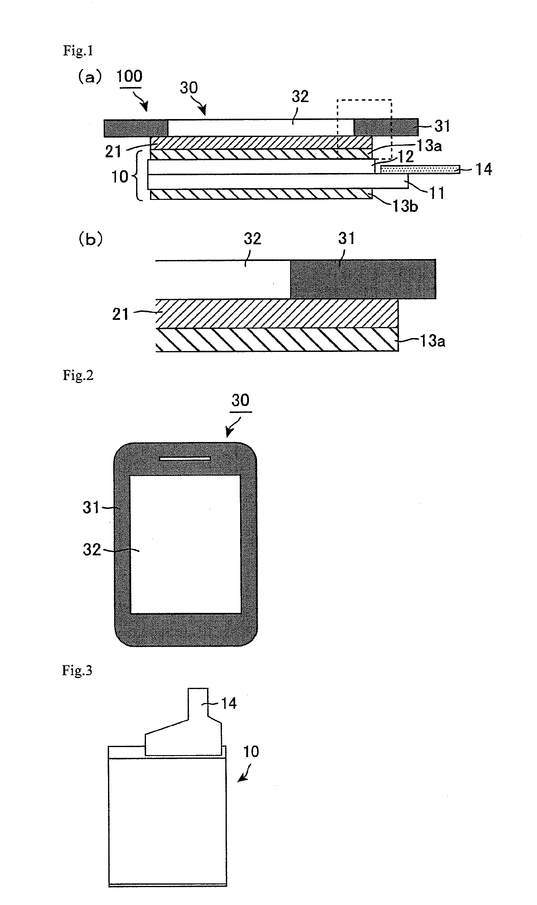
[0040]FIGS. 1 are a schematic cross-sectional view showing a display device of Embodiment 1. FIG. 1(a) is a general view. FIG. 1(b) is an enlarged view showing the area enclosed by the dot line in FIG. 1(a), that is, the vicinity of an end portion of an adhesive layer. FIG. 2 is a schematic plane view showing a cover substrate of Embodiment 1. FIG. 3 is a schematic plane view showing a liquid crystal display panel of Embodiment 1.
[0041]As shown in FIG. 1(a), a display panel 100 of the present embodiment includes: a liquid crystal display panel 10; a cover substrate 30 disposed on the display side of the liquid crystal display panel 10; an adhesive layer 21 interposed between the liquid crystal display panel 10 and the cover substrate 30; a backlight unit (not shown) disposed on the back side of the liquid crystal display panel 10; and a cabinet (not shown) for holding these components. In the display device 100, the liquid crystal display panel 10 and the cover substrate 30 are bond...
embodiment 2
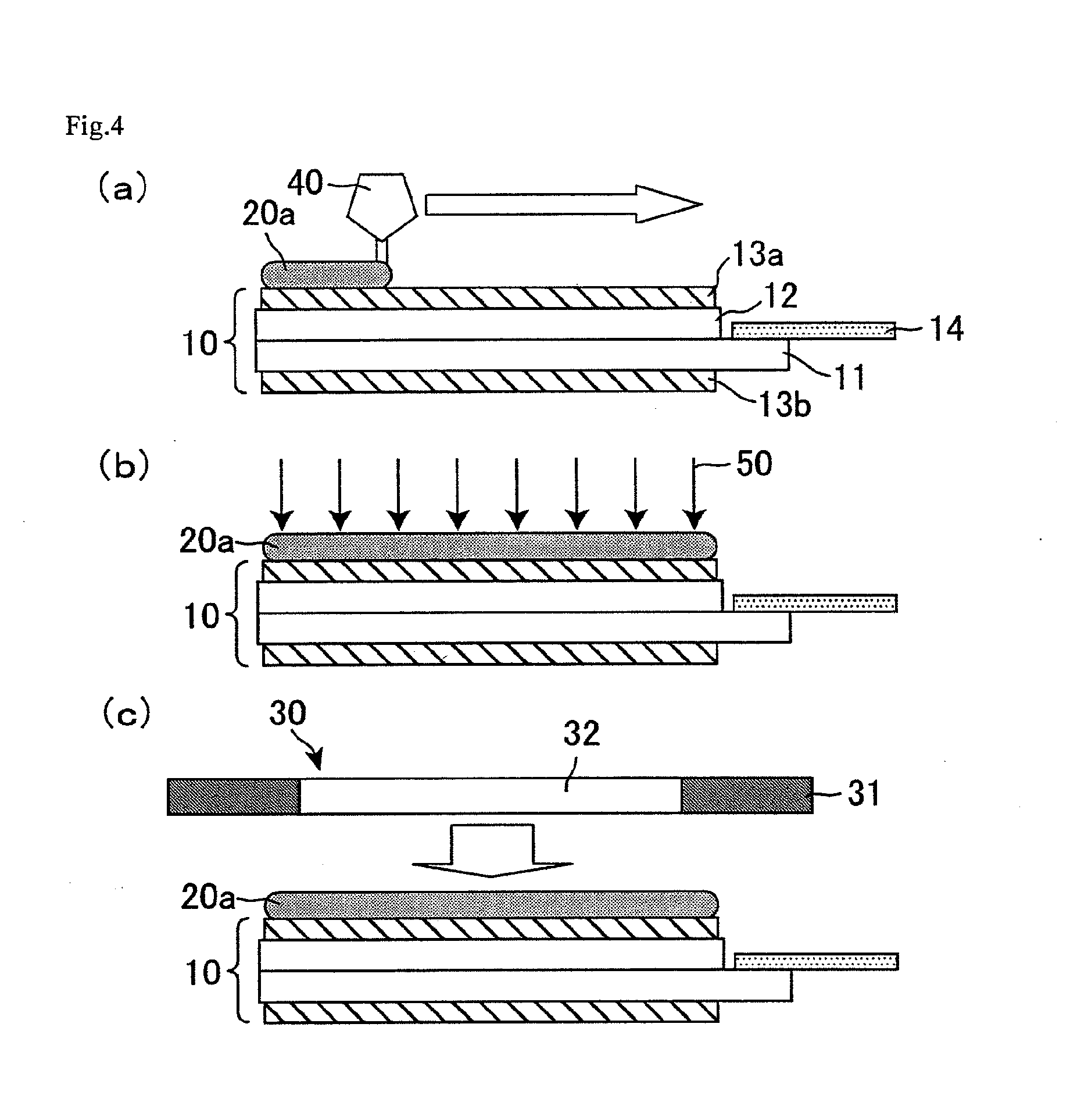
[0071]The following will describe the display device of Embodiment 2 referring to FIG. 5. The contents of Embodiment 2 overlapping with those of Embodiment 1 are not described here.
[0072]The display device of the present embodiment has the same structure as that of Embodiment 1. Further, the adhesive layer of the present embodiment contains a radically polymerized resin in addition to the cationically polymerized resin. The radically polymerized resin is formed by chain polymerization of monomers or oligomers with a radical serving as an active species. A radical has a higher reactivity than a cation, and therefore the radically polymerized resin is formed by entire curing in a shorter time period than the cationically polymerized resin is. Thus, the adhesive, which is a material of the adhesive layer, of the present embodiment is cured in a shorter time period than in Embodiment 1, so that the display device is produced in better productivity.
[0073]The following will describe a met...
embodiment 3
[0082]The following will describe the display device of Embodiment 3 referring to FIG. 6. The contents of Embodiment 3 overlapping with those of Embodiment 1 are not described here.
[0083]The display device of the present embodiment has the same structure as that of Embodiment 1. Further, the adhesive layer of the present embodiment contains a cationically polymerized resin formed by thermal curing. Thus, the adhesive, which is a material of the adhesive layer, of the present embodiment is more rapidly cured by heating. This results in a shorter curing time period of the adhesive, which is a material of the adhesive layer, and better productivity in the present embodiment than in Embodiment 1.
[0084]The following will describe a method for producing the display device of Embodiment 3 referring to FIG. 6. FIGS. 6(a) to 6(d) each are a schematic cross-sectional view showing the display device of Embodiment 3 in the production process.
[0085]In the same manner as in Embodiment 1, the liqu...
PUM
| Property | Measurement | Unit |
|---|---|---|
| refractive index | aaaaa | aaaaa |
| viscosity | aaaaa | aaaaa |
| haze | aaaaa | aaaaa |
Abstract
Description
Claims
Application Information