Solid-state imaging device, method of driving the same, and electronic system including the device

a solid-state imaging and imaging device technology, applied in the direction of television system scanning details, radioation control devices, television systems, etc., can solve the problems of difficult to eliminate the fluctuations of reset voltage vdd and thermal noise, and difficult to eliminate the noise occurring for each reset operation, so as to suppress image quality deterioration, and reduce random noise and unevenness

Inactive Publication Date: 2010-12-09
SONY CORP
View PDF5 Cites 35 Cited by
  • Summary
  • Abstract
  • Description
  • Claims
  • Application Information

AI Technical Summary

Benefits of technology

[0021]As described above, in the case of employing a drive method in which reset operation is performed to eliminate noise after the signal level is read out, while it is possible to eliminate offset noise occurring fixedly, it is difficult to eliminate noise occurring for each reset operation. For example, it is difficult to eliminate fluctuations of the reset voltage Vdd and thermal noise.
[0022]Accordingly, it is desirable to provide a solid-state imaging device, a method of driving the device, and an electronic system capable reducing random noise and unevenness on the screen at reset time in the case of driving to read out the reset level after reading out the signal level, and reducing deterioration of the image quality at the time of reset operation.
[0025]In using a drive method in which the reset level is read out after reading out the signal level, it is necessary to have a structure in which at least a part of a reset-transistor side of the impurity-diffusion region has a low impurity concentration in order for the pixel structure of a unit pixel to have a depleted reset-transistor side of the impurity-diffusion region. Thereby, it is possible to reduce random noise and unevenness on the screen (luminance unevenness on the screen) at the time of resetting the impurity-diffusion region.
[0026]And during an on period of the reset transistor, the voltage of the voltage supply line, that is to say, the drain voltage of the reset transistor is changed from the first voltage to the second voltage. Thereby, the voltage of the impurity-diffusion region converges to a voltage determined by the depletion potential without being influenced by an initial value of the potential of the impurity-diffusion region. As a result, it is possible to suppress image-quality deterioration caused by residual images of the image-quality deterioration at reset operation time (residual images dependent on the initial state).
[0027]By the present invention, in the case of driving in which a reset level is read out after the readout of a signal level, it is possible to reduce random noise and unevenness of the screen at reset time, and to reduce image-quality deterioration at the time of reset operation.

Problems solved by technology

As described above, in the case of employing a drive method in which reset operation is performed to eliminate noise after the signal level is read out, while it is possible to eliminate offset noise occurring fixedly, it is difficult to eliminate noise occurring for each reset operation.
For example, it is difficult to eliminate fluctuations of the reset voltage Vdd and thermal noise.

Method used


Image

  • Solid-state imaging device, method of driving the same, and electronic system including the device
  • Solid-state imaging device, method of driving the same, and electronic system including the device
  • Solid-state imaging device, method of driving the same, and electronic system including the device

Examples


first embodiment

2. First Embodiment

[0110]A first embodiment according to the present invention is made such that at the time of readout driving of a reset level after readout of a signal level, random noise and unevenness on a screen are reduced at reset time, and image quality deterioration caused by a residual-image phenomenon at reset operation time is reduced.

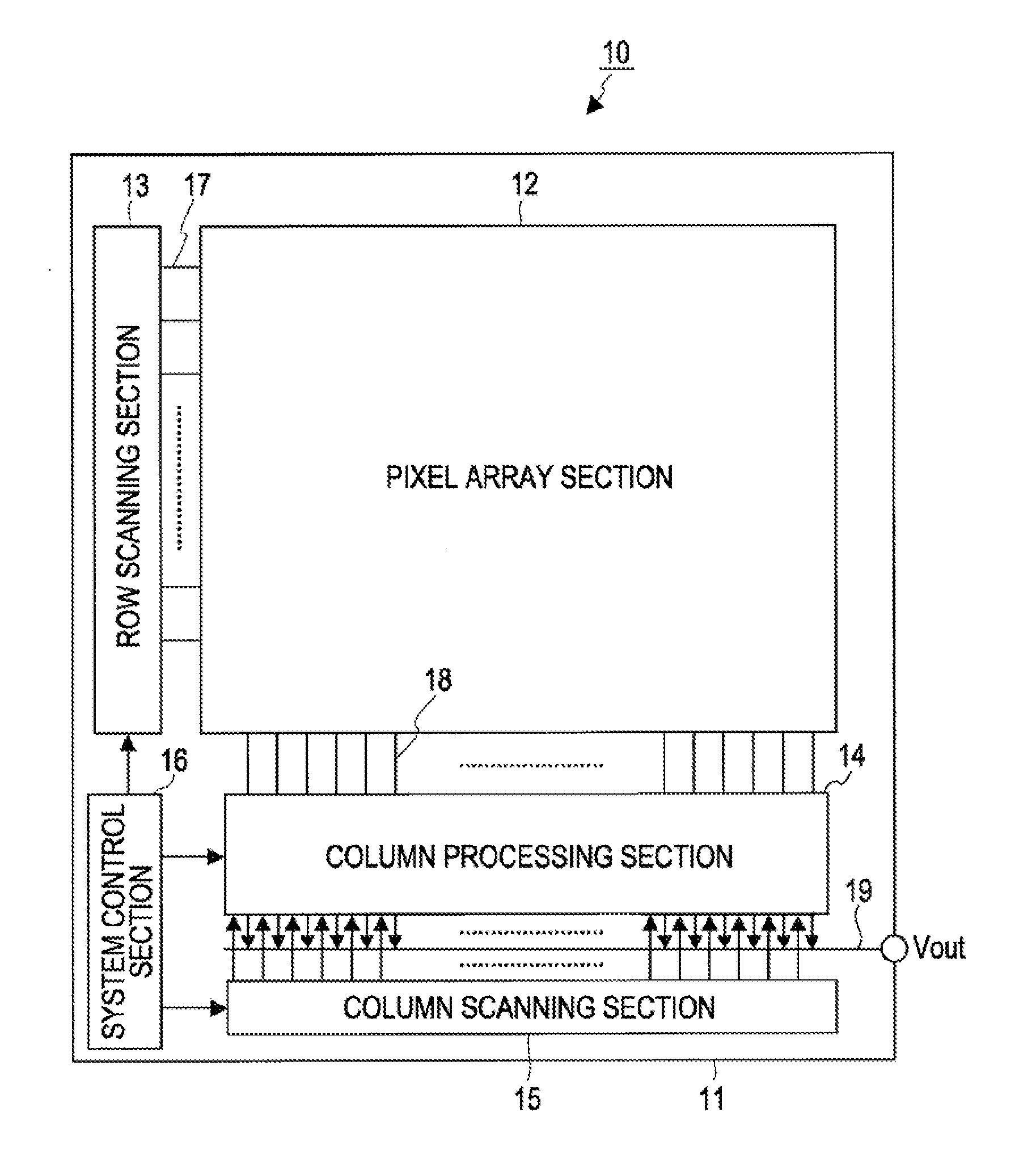
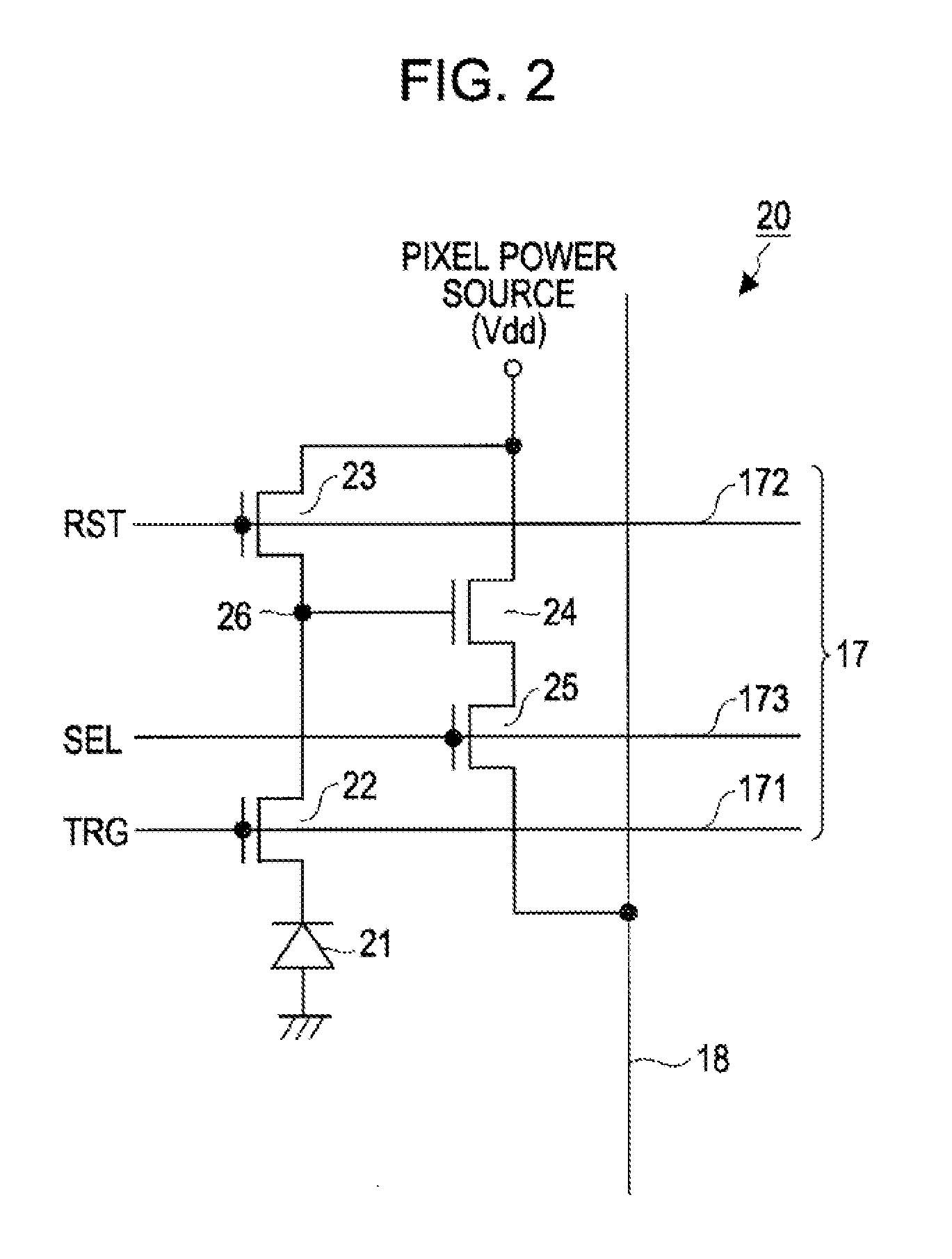
[0111]For that purpose, in the first embodiment, the CMOS image sensor 10 in FIG. 1 has a drive circuit which changes the drain voltage VRD of the reset transistor 23 from a first voltage Vrstl to a second voltage Vrst while the reset transistor 23 is on. This drive circuit corresponds to the row scanning section 13 driving each pixel 20 of the pixel array section 12 for each row.

[0112]Here, the drain voltage VRD of the reset transistor 23 is a reset voltage resetting the FD section 26. Also, the first voltage Vrstl is a voltage lower than a depletion potential of a layer between the above-described reset transistor 23 and the FD section 2...

second embodiment

3. Second Embodiment

[0161]Incidentally, the total load of the drive circuit is different in the case of batch pixel driving and the row-sequentially pixel driving, and thus a rise time and a fall time of the signal transition of the reset pulse RST are different because of a fall of the power-source voltage, etc. This means that the active period of the reset pulse RST is different in the case of batch pixel driving and in the case of row-sequential pixel driving.

[0162]Here, in the timing chart in FIG. 29, the reset pulse RST in the case of batch pixel driving is a pulse in a first half, that is to say, the reset pulse for initialization before batch transfer. Also, the reset pulse RST in the case of row-sequential pixel driving is a pulse in a last half, that is to say, the reset pulse for re-initialization performed in a readout period. As described above, the timing chart in FIG. 29 show sequence of driving in the case of reading out the signal charge held in the FD section 26, o...


PUM


Abstract

A solid-state imaging device includes: a unit pixel including a photoelectric conversion section, an impurity-diffusion region capable of temporarily accumulating or holding electric charges generated by the photoelectric conversion section, and a reset transistor resetting the impurity-diffusion region by a voltage of a voltage-supply line, and having an impurity concentration such that at least the reset transistor side of the impurity-diffusion region becomes a depletion state; and a drive circuit changing the voltage of the voltage-supply line from a first voltage lower than a depletion potential of the reset transistor side of the impurity-diffusion region to a second voltage higher than the depletion potential while the reset transistor is on.

Description

BACKGROUND OF THE INVENTION[0001]1. Field of the Invention[0002]The present invention relates to solid-state imaging devices, methods of driving the solid-state imaging devices, and electronic systems.[0003]2. Description of the Related Art[0004]In a general solid-state imaging device, when electric charges generated by photoelectric conversion are read, the charges are accumulated in an impurity-diffusion region called a floating-diffusion region, or the charges are transferred from a light receiving section to the impurity-diffusion region so that the charges are converted into a voltage in that impurity-diffusion region. A pixel in such a kind of solid-state imaging device generally has a configuration including a reset transistor which resets the floating-diffusion region (hereinafter referred to as an “FD section”) to have a predetermined potential.[0005]In a pixel configuration having a reset transistor, the reset transistor is set to be an on state, and the FD section is init...

Claims


Application Information

Patent Timeline
Patent Type & Authority Applications(United States)
IPC IPC(8): H04N5/335H01L27/146H04N5/357H04N5/363H04N5/369H04N5/374H04N5/376
CPCH01L27/14609H01L27/14643H04N5/3741H04N5/3597H04N5/363H04N5/35527H04N25/575H04N25/626H04N25/65H04N25/766H04N25/00
Inventor OIKE, YUSUKE
Owner SONY CORP
Why Eureka
Try Eureka