

Method of forming carbon-containing layer
- Summary
- Abstract
- Description
- Claims
- Application Information
AI Technical Summary
Benefits of technology
Problems solved by technology
Method used
Image

Examples
first embodiment
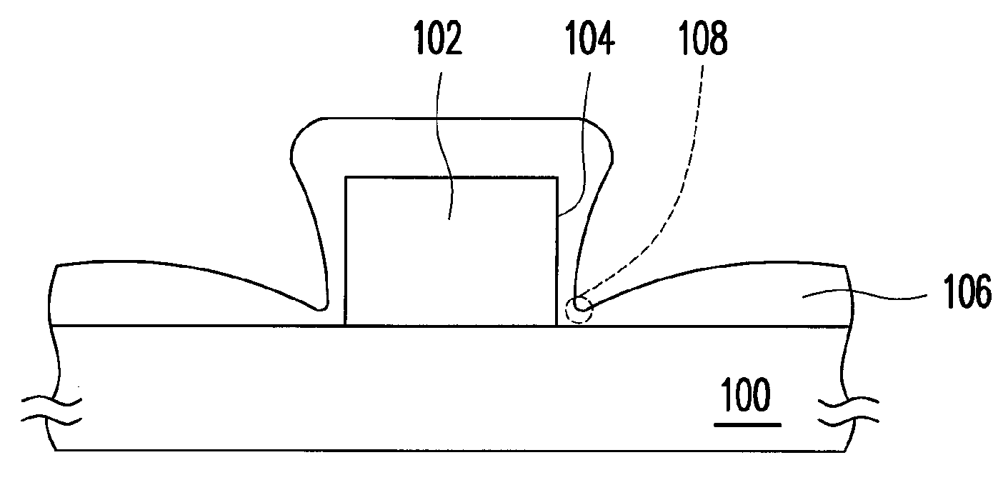
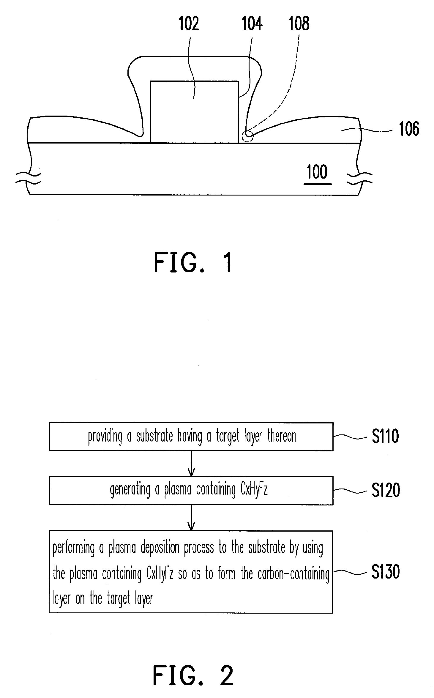
[0027]FIG. 2 is a schematic flow chat of the method of forming a carbon-containing layer according to an embodiment of the present invention. FIG. 3 is a schematic cross-sectional view of a carbon-containing layer according to a first embodiment of the present invention. In the present embodiment, the carbon-containing layer is used as a hard mask layer, for example.
[0028]As shown in FIGS. 2 and 3, first, a step S110 is performed. A substrate 200 is provided and a target layer 202 has been formed on the substrate 200. The substrate 200 is, for example, a silicon substrate. The target layer 202 is, for example, a protruding structure and has a sidewall 206 substantially perpendicular to the surface 204 of the substrate 200. A material of the target layer 202 may be a dielectric material or a conductive layer.
[0029]Next, referring to FIG. 2, the step S120 is performed. A plasma containing CxHyFz is generated, wherein x is from about 1 to 8, y is from about 1 to 10 and z is from about ...
second embodiment
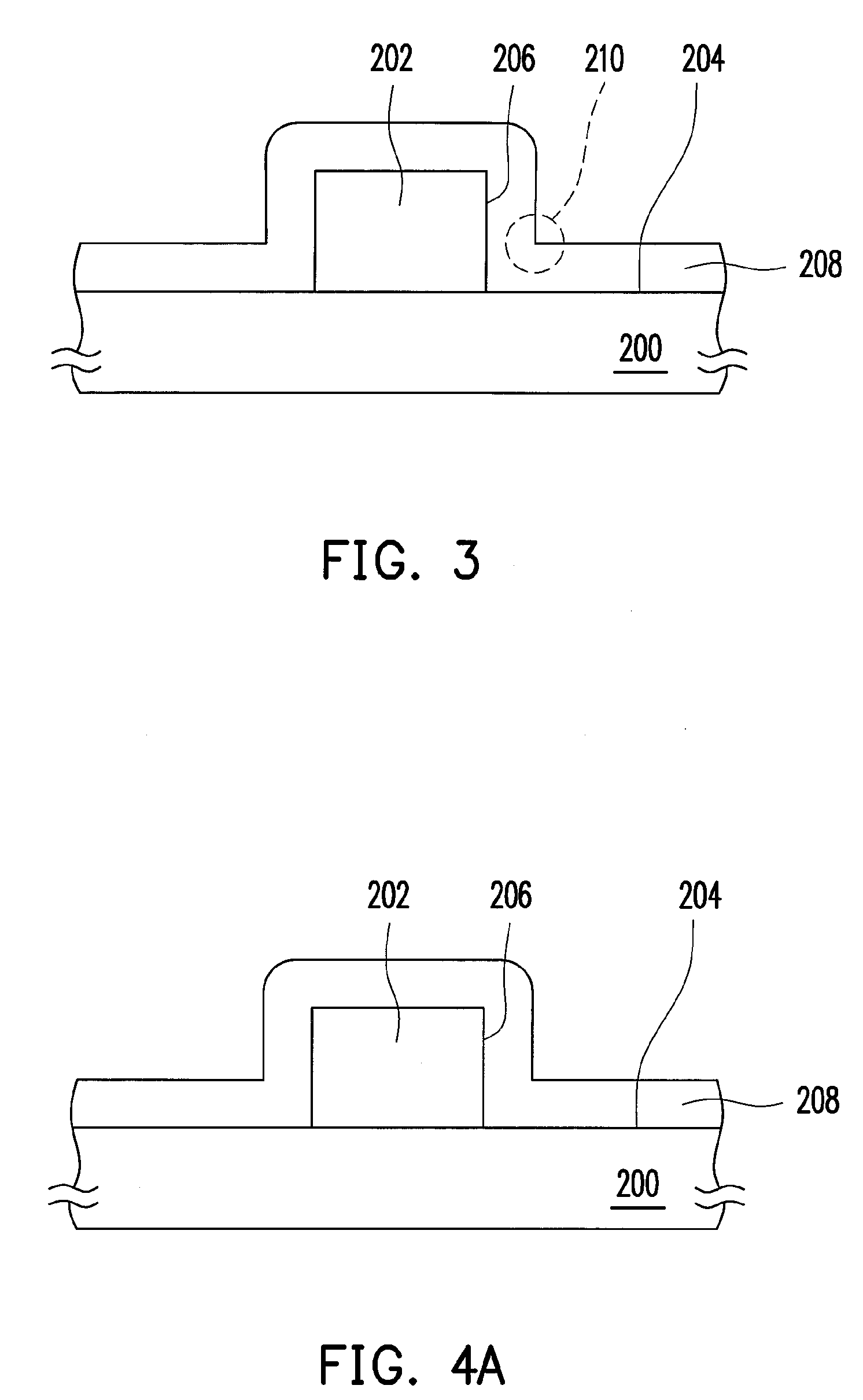
[0033]FIGS. 4A through 4B are schematic cross-sectional views showing the steps of a method of forming a carbon-containing layer according to a second embodiment of the present invention.
[0034]As shown in FIG. 2 and FIG. 4A, first, a step S110 is performed. A substrate 200 is provided and a target layer 202 has been formed on the substrate 200. The substrate 200 is, for example, a silicon substrate. The target layer 202 is, for example, a gate structure and includes a sidewall 206 substantially perpendicular to the surface 204 of the substrate 200.
[0035]Next, referring to FIG. 2, the step S120 is performed. A plasma containing CxHyFz is generated. The process parameters of the method for generating the plasma containing CxHyFz are referred to the description of the first embodiment, and are not iterated herein.
[0036]Thereafter, referring to FIG. 2 and FIG. 4A, the step S130 is implemented. A plasma deposition process is performed to the substrate 200 by using the plasma containing C...
third embodiment
[0040]FIG. 5 is a schematic cross-sectional view of a carbon-containing layer according to a third embodiment of the present invention.
[0041]As shown in FIG. 2 and FIG. 5, first, a step S110 is performed. A substrate 200 is provided and a target layer 202 has been formed on the substrate 200. The substrate 200 is, for example, a silicon substrate. The target layer 202 may be a dielectric material layer or a conductive material layer with a flat surface.
[0042]Next, referring to FIG. 2, the step S120 is performed. A plasma containing CxHyFz is generated. The process parameters of the method for generating the plasma containing CxHyFz are referred to the descriptions of the first embodiment, and are not iterated herein.
[0043]Thereafter, referring to FIG. 2 and FIG. 5, the step S130 is implemented. A plasma deposition process is performed to the substrate 200 by using the plasma containing CxHyFz so as to form the carbon-containing layer 208 on the target layer 202. In the step S130, th...
PUM
 Abstract
Description
Claims
Application Information