Interconnect Structures Having Lead-Free Solder Bumps

Active Publication Date: 2010-12-16
TAIWAN SEMICON MFG CO LTD
View PDF16 Cites 22 Cited by
  • Summary
  • Abstract
  • Description
  • Claims
  • Application Information

AI Technical Summary

Benefits of technology

[0010]The advantageous features of the embodiments in

Problems solved by technology

However, lead is a toxic material, and legislation and industry requirements have demanded lead-free solder bumps.
Unfortunately, the commonly known lead-free solders, such as Sn—Ag and Sn—Ag—Cu, are too brittle, and suffer from cracking Further, the lead-free bumps are rigid, and could induce delamination and cracking in dielectric layers.
In integrated circuits formed using advanced technologies, the bump cracking and ELK de

Method used


Image

  • Interconnect Structures Having Lead-Free Solder Bumps
  • Interconnect Structures Having Lead-Free Solder Bumps

Examples


Embodiment Construction

[0013]The making and using of the embodiments of the present invention are discussed in detail below. It should be appreciated, however, that the embodiments provide many applicable inventive concepts that can be embodied in a wide variety of specific contexts. The specific embodiments discussed are merely illustrative of specific ways to make and use the invention, and do not limit the scope of the invention.

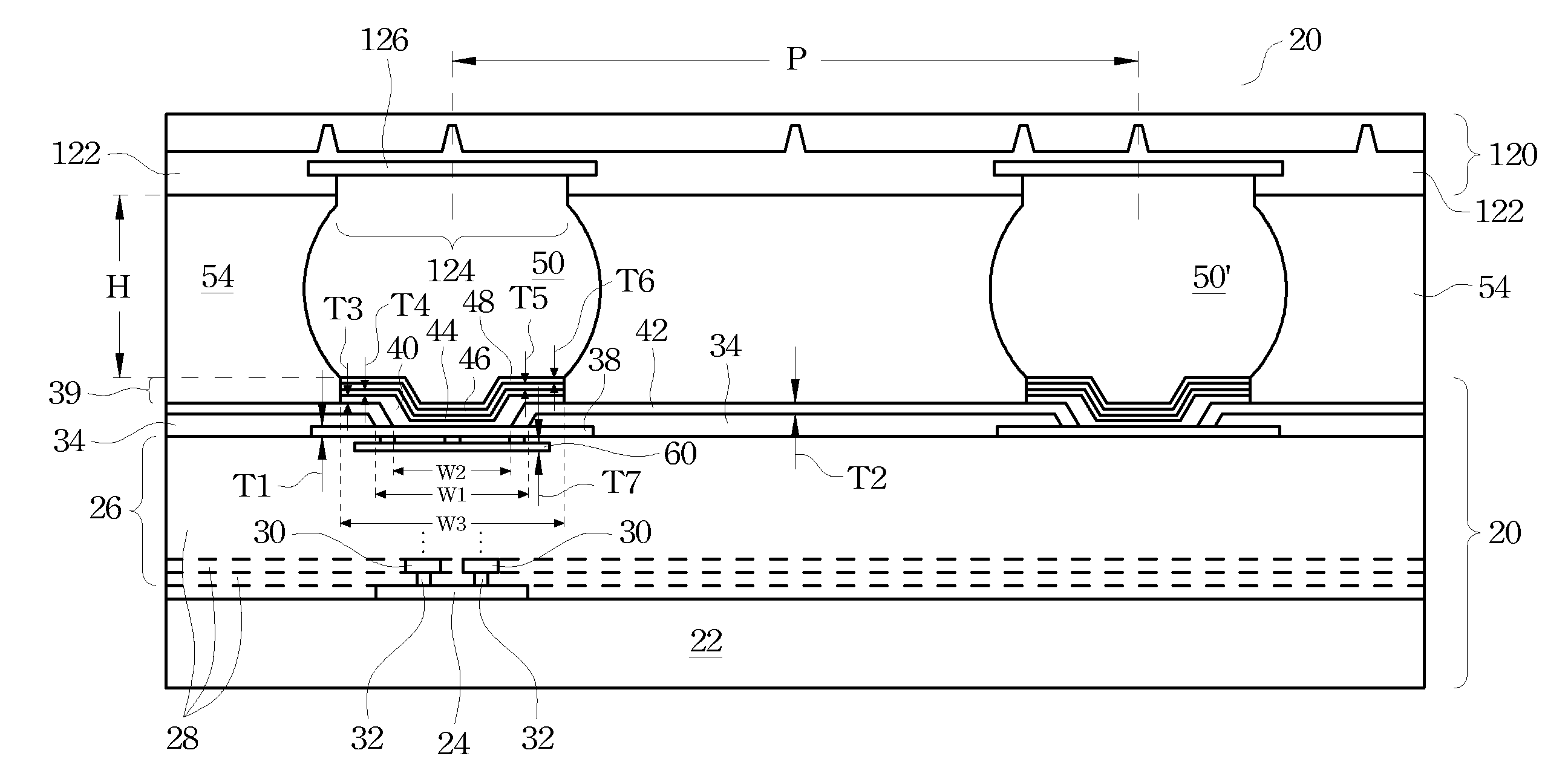
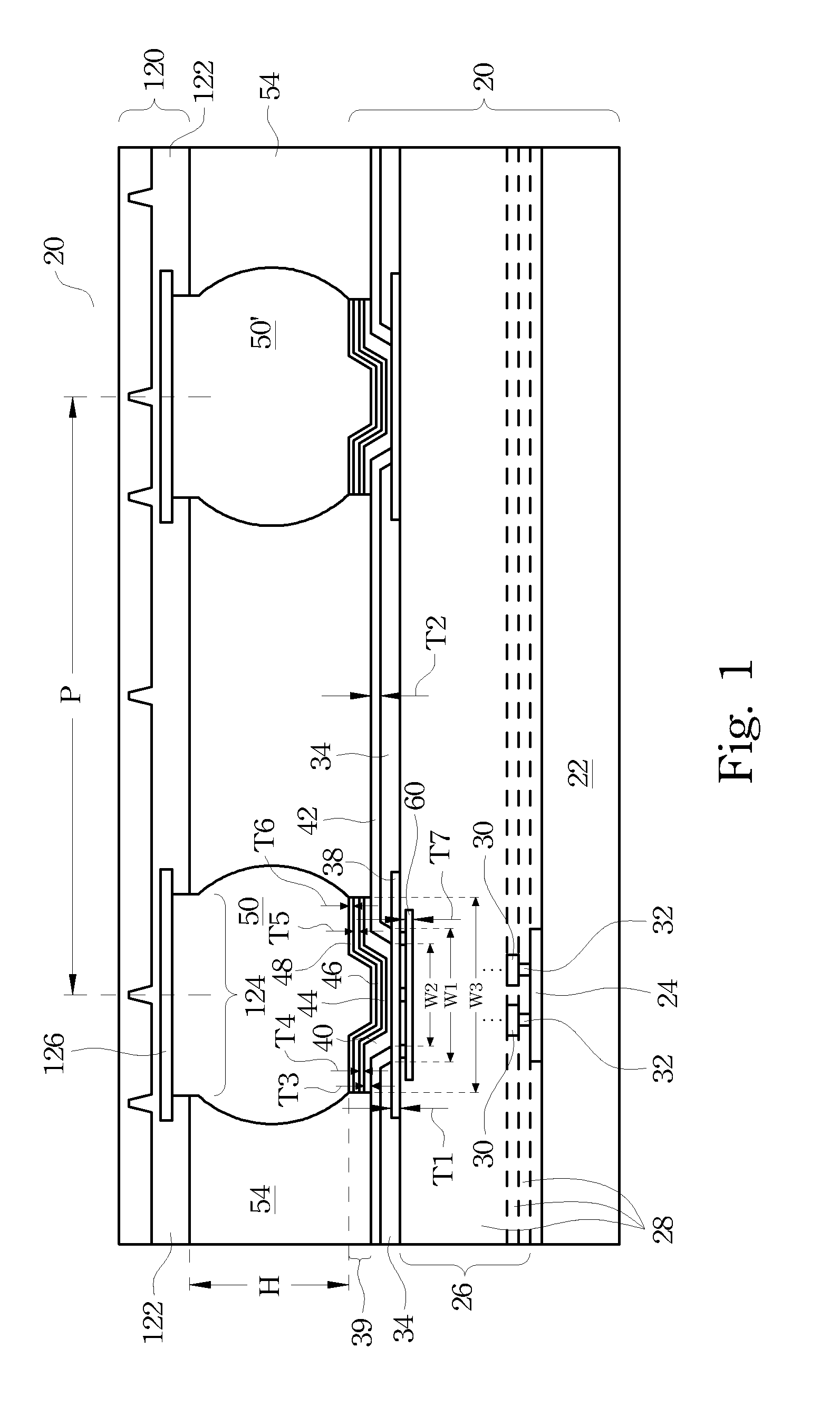
[0014]FIG. 1 illustrates a cross-sectional view of a portion of chip (or wafer) 20, which includes substrate 22, on which active circuit 24 is formed. Chip / wafer 20 is bonded to package substrate 120 through solder bumps 50 and 50′. Substrate 22 may be a semiconductor substrate formed of commonly used semiconductor materials, such as silicon, silicon germanium, or the like. Active circuit 24, which is symbolized using a rectangle, is formed at the surface of substrate 22, and may include complementary metal-oxide-semiconductor (CMOS) transistors, resistors, capacitors, and the ...


PUM


Abstract

An integrated circuit structure includes a semiconductor substrate, and a polyimide layer over the semiconductor substrate. An under-bump-metallurgy (UBM) has a first portion over the polyimide layer, and a second portion level with the polyimide layer. A first solder bump and a second solder bump are formed over the polyimide layer, with a pitch between the first solder bump and the second solder bump being no more than 150 μm. A width of the UBM equals one-half of the pitch plus a value greater than 5 μm.

Description

[0001]This application claims the benefit of U.S. Provisional Application No. 61 / 187,542 filed on Jun. 16, 2009, entitled “Interconnect Structures Having Lead-Free Solder Bumps,” which application is hereby incorporated herein by reference.TECHNICAL FIELD[0002]This invention relates generally to integrated circuits, and more particularly to the structure and formation methods of bonding structures of integrated circuits.BACKGROUND[0003]Integrated circuit (IC) chips are often electrically connected to package substrates in packaging assemblies to provide external signal exchange. A commonly used bonding scheme is flip-chip bonding. Flip-chips provide the most rugged mechanical interconnection. When underfilled with an adhesive, such as an epoxy, flip-chips can withstand rugged durability tests. Additionally, flip-chip bonding is a low-cost interconnection scheme suitable for high-volume automated production.[0004]Flip-chips are typically made by placing solder bumps on silicon chips....

Claims


Application Information

Patent Timeline
IPC IPC(8): H01L23/498
CPCH01L24/05H01L24/12H01L24/16H01L2224/056H01L2224/13023H01L2224/131H01L2224/29111H01L2924/01013H01L2924/01014H01L2924/01015H01L2924/01022H01L2924/01028H01L2924/01029H01L2924/01047H01L2924/0105H01L2924/01074H01L2924/01079H01L2924/01082H01L2924/01322H01L2924/014H01L2924/05042H01L2924/14H01L2924/19041H01L2924/19043H01L2924/00014H01L2924/01006H01L2924/01019H01L2924/01033H01L2924/01075H01L2224/05027H01L2224/0558H01L2224/05022H01L2224/05572H01L2924/10253H01L2924/00H01L2224/0401H01L2924/0002H01L2224/05552H01L2224/16237
Inventor LII, MIRNG-JILEE, CHIEN-HSIUNYU, CHEN-HUAJENG, SHIN-PUUKU, CHIN-YU
Owner TAIWAN SEMICON MFG CO LTD
Why Eureka
Try Eureka