

Display device and method for driving display
a technology of display device and display device, which is applied in the direction of digital storage, instruments, computing, etc., can solve the problems of difficult to reliably sink the gate line voltage down, insufficient sink-down tft, and serious shift of threshold voltage, so as to reduce the “on” duty cycle
- Summary
- Abstract
- Description
- Claims
- Application Information
AI Technical Summary
Benefits of technology
Problems solved by technology
Method used
Image

Examples
first embodiment
[0113]FIG. 10 shows the configuration of a liquid crystal display device 1 that is a first display device according to the present embodiment.
[0114]The liquid crystal display device 1 includes a display panel 2, a flexible printed circuit board 3, and a control board 4.
[0115]The display panel 2 is an active matrix display panel arranged such that, using amorphous silicon, polycrystalline silicon, CG silicon, microcrystalline silicon, or the like silicon, a display region 2a, a plurality of gate lines (scan signal lines) GL, a plurality of source lines (data signal lines) SL, and gate drivers (scan signal line driving circuits) 5a and 5b are built onto a glass substrate. The display region 2a is a region where a plurality of pixels PIX are arranged in a matrix manner. Each of the pixels PIX includes a TFT 21 that is a selection element of a pixel, a liquid crystal capacitor CL, and an auxiliary capacitor Cs. A gate of the TFT 21 is connected to the gate line GL, and a source of the T...
second embodiment
[0144]A second display device according to the present embodiment is different from the liquid crystal display device 1 shown in FIG. 10 in that the shift registers of the gate drivers 5a and 5b are differently configured.
[0145]The respective configurations of the gate drivers 5a and 5b in such a case are shown in FIG. 4.
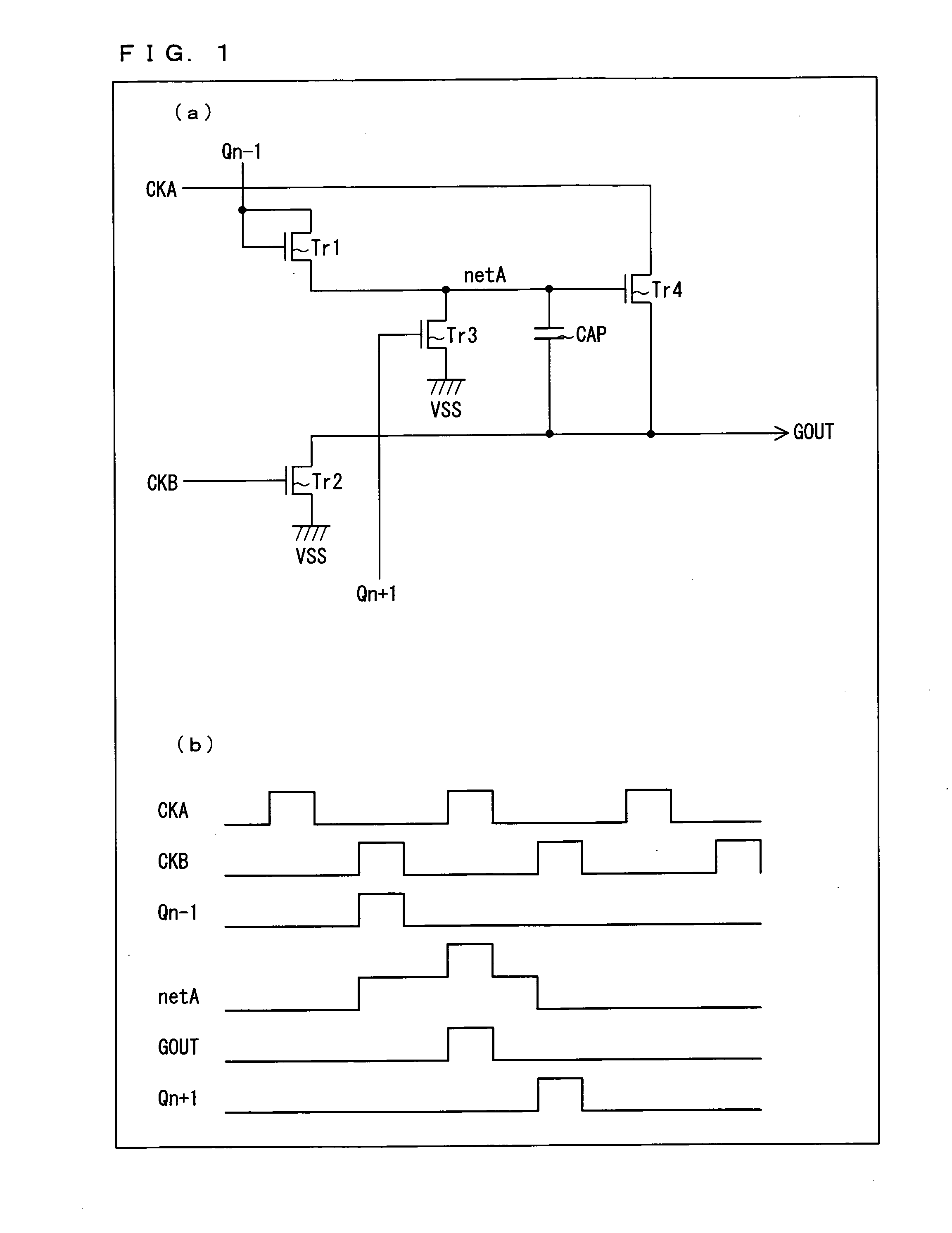
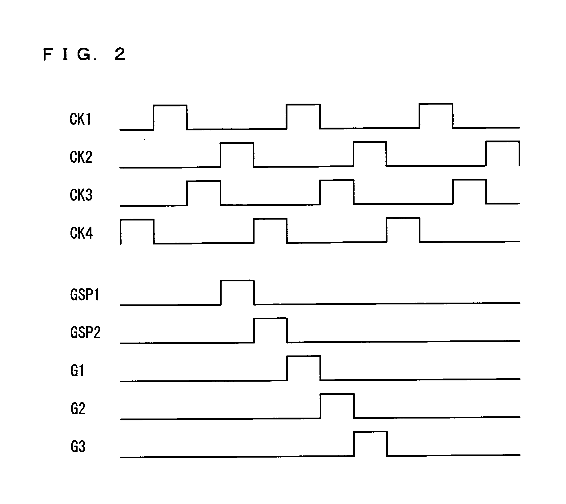
[0146]The gate driver 5a includes a first shift register 52a having a plurality of cascaded shift register stages SR (SR1, SR3, SR5, . . . ) therein. Each of the shift register stages SR includes a set input terminal Qn−1, an output terminal GOUT, a reset input terminal Qn+1, clock input terminals CKA, CKB, CKC, CKD, and a Low power source input terminal VSS. From the control board 4 are supplied a clock signal (first clock signal) CK1, a clock signal (second clock signal) CK2, a clock signal (third clock signal) CK3, a clock signal (fourth clock signal) CK4, a gate start pulse (shift pulse) GSP1, and Low power source VSS (For convenience of explanation, the same re...
third embodiment
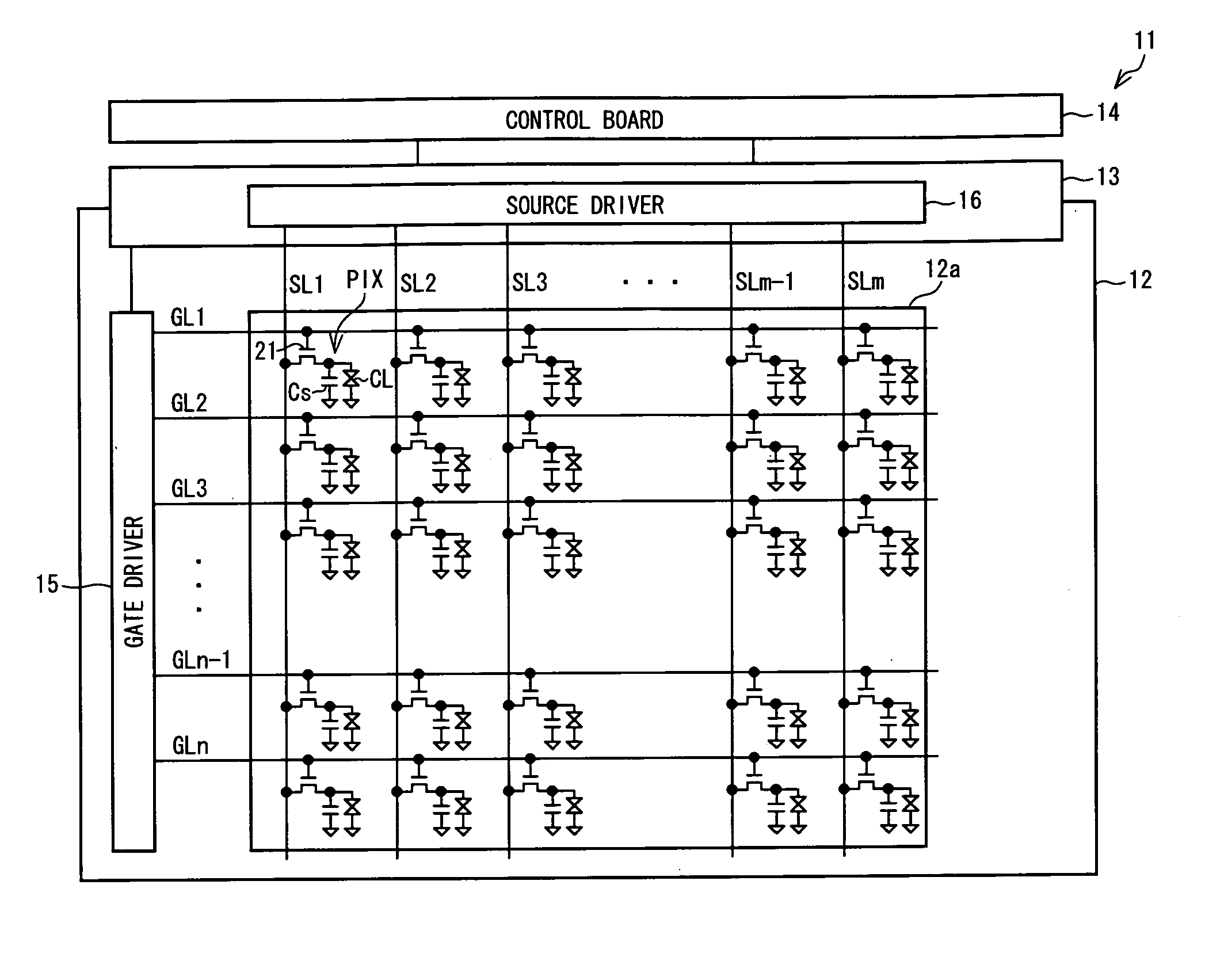
[0172]FIG. 11 shows the configuration of a liquid crystal display device 11 that is a third display device according to the present embodiment.
[0173]The liquid crystal display device 11 includes a display panel 12, a flexible printed circuit board 13, and a control board 14.
[0174]The display panel 12 is an active matrix display panel arranged such that, using amorphous silicon, polycrystalline silicon, CG silicon, microcrystalline silicon, or the like silicon, a display region 12a, a plurality of gate lines (scan signal lines) GL, a plurality of source lines (data signal lines) SL, and gate drivers (scan signal line driving circuits) 15 are built onto a glass substrate. The display region 12a is a region where a plurality of pixels PIX are arranged in a matrix manner. Each of the pixels PIX includes a TFT 21 that is a selection element of a pixel, a liquid crystal capacitor CL, and an auxiliary capacitor Cs. A gate of the TFT 21 is connected to the gate line GL, and a source of the ...
PUM
 Abstract
Description
Claims
Application Information