Silicon-on-insulator (SOI) six-transistor static random access memory (SRAM) unit and fabrication method thereof

A six-transistor and manufacturing method technology, applied in the field of memory design and manufacturing, can solve the problems of large occupied area of ​​SRAM cells, weak anti-noise capability, poor stability, etc., and achieve the effects of simple manufacturing process, improved anti-noise capability, and shortened cycle.

Inactive Publication Date: 2017-07-14
SHANGHAI INST OF MICROSYSTEM & INFORMATION TECH CHINESE ACAD OF SCI
View PDF5 Cites 1 Cited by
  • Summary
  • Abstract
  • Description
  • Claims
  • Application Information

AI Technical Summary

Problems solved by technology

[0007] In view of the above-mentioned shortcomings of the prior art, the object of the present invention is to provide a SOI six-transistor SRAM unit and a manufacturing method thereof, which are used to solve the problems of large occupied area, poor stability, and leakage power of the SOI six-transistor SRAM unit in the prior art. The problem of high power consumption and weak anti-noise ability

Method used


Image

  • Silicon-on-insulator (SOI) six-transistor static random access memory (SRAM) unit and fabrication method thereof
  • Silicon-on-insulator (SOI) six-transistor static random access memory (SRAM) unit and fabrication method thereof
  • Silicon-on-insulator (SOI) six-transistor static random access memory (SRAM) unit and fabrication method thereof

Examples


Embodiment 1

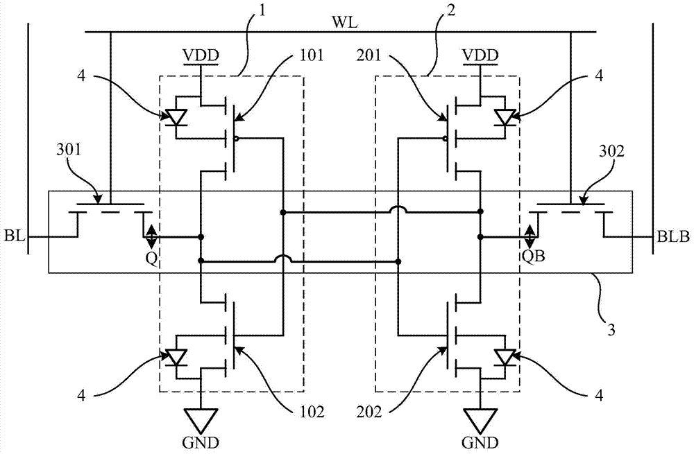
[0096] The present invention provides a SOI six-transistor SRAM unit, please refer to figure 1 , shown as a schematic circuit diagram of the SOI six-transistor SRAM cell, including:

[0097] The first inverter 1 is composed of a first PMOS transistor 101 and a first NMOS transistor 102;

[0098] The second inverter 2 is composed of a second PMOS transistor 201 and a second NMOS transistor 202;

[0099] The acquisition transistor 3 is composed of a third NMOS transistor 301 and a fourth NMOS transistor 302; the source of the third NMOS transistor 301 is connected to the output terminal of the first inverter and the input of the second inverter terminal, the gate is connected to the word line WL of the memory, and the drain is connected to the bit line BL of the memory; the source of the fourth NMOS transistor 302 is connected to the output end of the second inverter and the first inverter The gate is connected to the word line of the memory, and the drain is connected to the ...

Embodiment 2

[0112] The present invention also provides a method for manufacturing an SOI six-transistor SRAM unit, comprising the following steps:

[0113] Step S1 is first performed: provide an SOI substrate including a back substrate, an insulating buried layer, and a top layer of silicon in sequence from bottom to top, and form a shallow trench isolation structure in the top layer of silicon to define an active region.

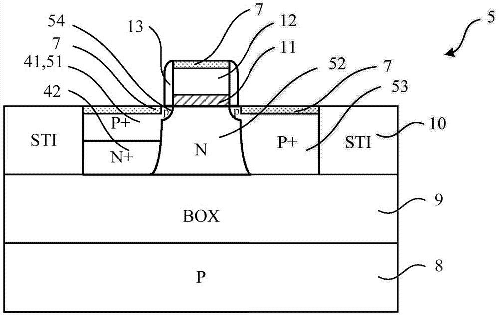
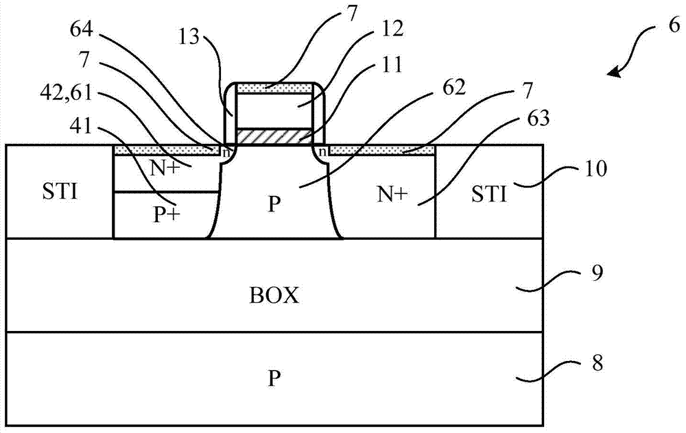
[0114] As an example, such as Figure 7 As shown, four active regions 20a, 20b, 20c, and 20d are defined. These four active regions are arranged in parallel in turn, and shallow trenches are formed around each active region, and the shallow trenches are filled with insulating materials to form shallow trenches. isolation structure. In this embodiment, the insulating material is silicon dioxide.

[0115] Then execute step S2: as Figure 8 As shown, an N well 30, a first P well 40a, and a second P well 40b are fabricated in the top layer silicon according to the posit...


PUM


Abstract

The invention provides a silicon-on-insulator (SOI) six-transistor static random access memory (SRAM) unit and a fabrication method thereof. The unit comprises a first phase inverter, a second phase inverter and an acquisition tube, wherein the first phase inverter comprises a first P-channel metal oxide semiconductor (PMOS) transistor and a first N-channel metal oxide semiconductor (NMOS) transistor, the second phase converter comprises a second PMOS transistor and a second NMOS transistor, and the acquisition tube comprises a third NMOS transistor and a fourth NMOS transistor. In the SOI six-transistor SRAM unit, tunneling diode structures are embedded into sources of the four transistors forming the first phase inverter and the second phase inverter, power consumption leakage and threshold voltage drift of the transistors caused by a floating body effect and a parasitic triode effect in a partially-depleted (PD) SOI device can be effectively suppressed on the condition of no increase on device area, and the noise resistant capability of the unit is improved; moreover, the fabrication method also has the advantages of simple manufacturing process and the like, and is completely compatible with an existing logic process; and a central symmetric structure and a sharing structure between units are employed in the unit, so that a storage array is convenient to form, and the design period of an SRAM chip is favorably shortened.

Description

technical field [0001] The invention belongs to the field of memory design and manufacture, and relates to an SOI six-transistor SRAM unit and a manufacturing method thereof. Background technique [0002] Since the invention of SOI technology in the 1980s, it has small parasitic capacitance, low power consumption, fast speed and natural anti-Single-Event-Latchup (SEL) ability compared with ordinary bulk silicon technology, making SOI The technology is very suitable for working in System-on-Chips (SoC), low power consumption and radiation resistance; in addition, Static Random Access Memory (SRAM) is widely used in consumer electronics, automotive electronics, processing Therefore, applying SOI technology to SRAM design has certain advantages. [0003] According to the degree of depletion of the MOS tube body region, SOI can be further divided into fully depleted (Full-Depleted, FD) SOI and partially depleted (Partially-Depleted, FD) SOI. For partially depleted SOI technolo...

Claims


Application Information

Patent Timeline
Patent Type & Authority Applications(China)
IPC IPC(8): H01L27/11H01L21/8244
CPCH10B10/00H10B10/12
Inventor 陈静何伟伟罗杰馨王曦
Owner SHANGHAI INST OF MICROSYSTEM & INFORMATION TECH CHINESE ACAD OF SCI
Why Eureka
Try Eureka