Single Electron Transistor Operating at Room Temperature and Manufacturing Method for Same

a single-electron transistor and room temperature technology, applied in the field of single-electron transistors, can solve the problems of difficult to improve the operating temperature of the device, difficult to intentionally control the height and width of the tunneling barrier, and the scale-down process of the semiconductor device resulting from the development of technology inevitably encounters a physical limit, so as to minimize the influence of the gate voltage on the tunneling barrier and effectively control only the electric potential

Active Publication Date: 2010-12-30
NANOCHIPS
View PDF3 Cites 8 Cited by
  • Summary
  • Abstract
  • Description
  • Claims
  • Application Information

AI Technical Summary

Benefits of technology

[0014]Accordingly, the present invention has been made in view of the above problems occurring in the conventional technology, and it is an object of the present invention to provide a single-electron transistor operating at room-temperature and a method of manufacturing the same. To be specific, the object of the present invention is to provide a single-electron transistor (SET) operating at room temperature and a method of manufacturing the same, which are capable of minimizing influence of the gate voltage on tunneling barriers and effectively controlling only the electric potential of a quantum dot (QD), by forming the quantum dot as an active channel using a trenched nano-wire structure and forming the gate to wrap most of the way around the quantum dot

Problems solved by technology

The scale-down process of the semiconductor devices resulting from the development of technology inevitably encounters a physical limit.
Such equipments with the high functionality require semiconductor devices with low power consumption, together with a high degree of integration density, because they require high power consumption.
1) The single-electron transistor requires a fine electrode structure in order to efficiently control electrons because it controls one electron using the physical property called Coulomb blockade which is enhanced in a nano-scale quantum dot.
2) The single-electron transistor must include a tunneling barrier between the quantum dot and the source (and also the drain) because it uses a tunneling phenomenon. The tunneling barrier is naturally formed by a pattern-dependant oxidation (PADOX) process when a gate oxide film is formed, making it difficult to intentionally control the height and width of the tunneling barrier. Although intentional tunneling barriers may be formed using a depletion gate, it is difficult to improve the operating temperature of the device because there is a limit in reducing a total capacitance of a quantum dot.
3) The gate is used to control the electric potential of a quantum dot. Here, a conventional single-electron transistor is operated only at low temperature because the tunneling barriers are influenced by the gate.
4) In particular, the gate is formed to cover the source and the drain region as well as the quantum dot. Thus, the gate voltage not only changes the electric potential of the quantum dot, but also influences the tunneling barriers formed on the left and right sides of the quantum dot.
5) When the gate voltage increases as described above, the height of the tunneling barriers is lowered. Consequently, the peak-to-valley current ratio (PVCR) characteristic of Coulomb oscillation is deteriorated.

Method used


Image

  • Single Electron Transistor Operating at Room Temperature and Manufacturing Method for Same
  • Single Electron Transistor Operating at Room Temperature and Manufacturing Method for Same
  • Single Electron Transistor Operating at Room Temperature and Manufacturing Method for Same

Examples


first embodiment

of the Present Invention

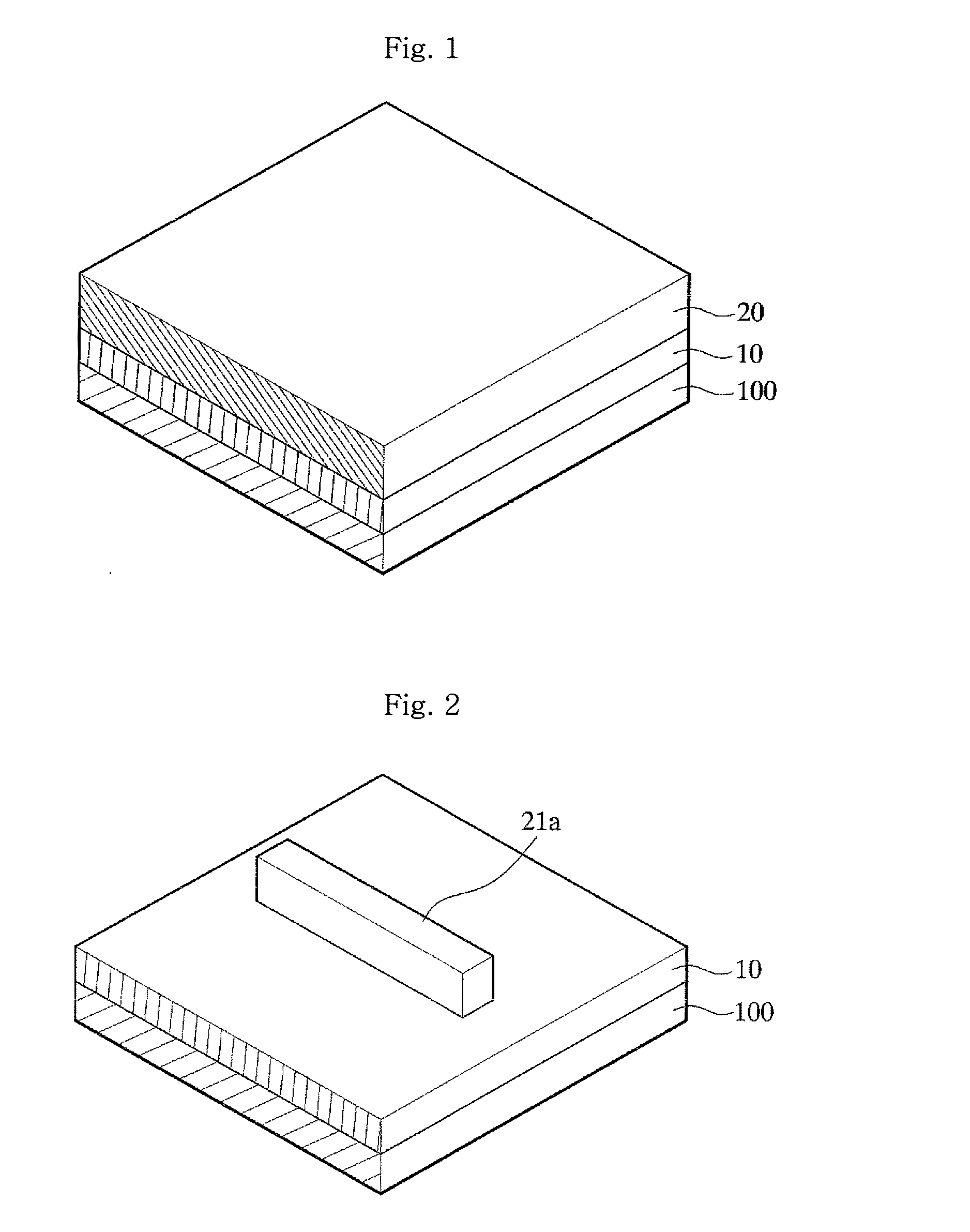
[0056]FIG. 2 is a partially sectional perspective view showing a state in which a nano-wire structure 21a according to a first embodiment of the present invention is formed. A first step is a step of forming the nano-wire structure 21a over the SOI substrate. The nano-wire structure 21a is formed by etching the top silicon layer 20. To this end, a resist is coated on the top silicon layer 20, a pattern is formed using a photolithography process or an electron-beam lithography process, and the top silicon layer 20 is etched using the formed pattern as a mask. The formed nano-wire structure can preferably have a width of 1 to 50 nm and a length of 1 to 1000 nm such that the total size of the transistor can be minimized.

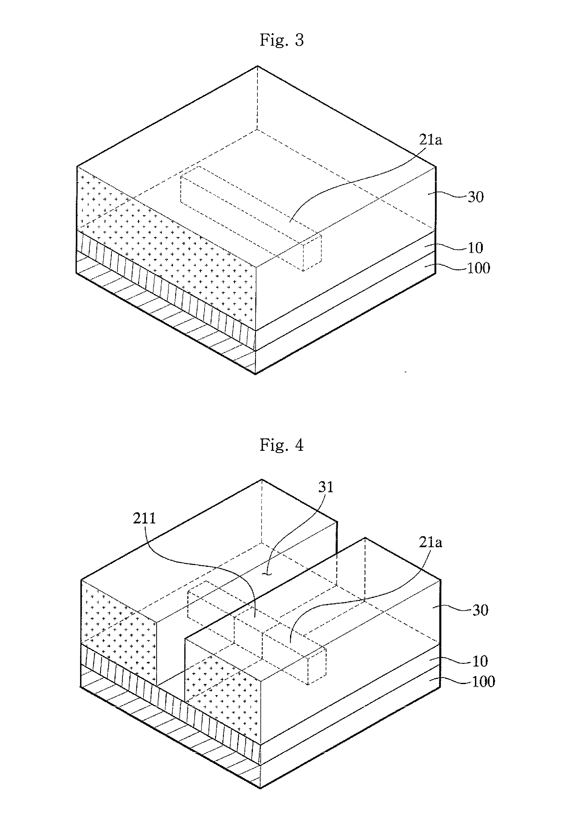
[0057]FIG. 3 is a partially sectional perspective view showing a state in which a second insulation film 30 is formed according to the first embodiment of the present invention. A second step is a step of forming the second insulation film 30 ove...

second embodiment

of the Present Invention

[0067]A first step according to the second embodiment of the present invention is a step of forming a nano-wire structure 21a. The first step of forming the nano-wire structure 21a preferably is identical with the first step of the first embodiment.

[0068]A second step according to the second embodiment of the present invention is a step of forming a second insulation film 30. The second step of forming the second insulation film 30 preferably is identical with the second step of the first embodiment.

[0069]A third step according to the second embodiment of the present invention is a step of forming a quantum dot 212. The third step of forming the quantum dot 212 preferably is identical with the third step of the first embodiment.

[0070]FIG. 17 is a partially sectional perspective view showing a state in which a metal film 50 is formed according to the second embodiment of the present invention. As shown in FIG. 17, a fourth step is a step of forming the metal f...

third embodiment

of the Present Invention

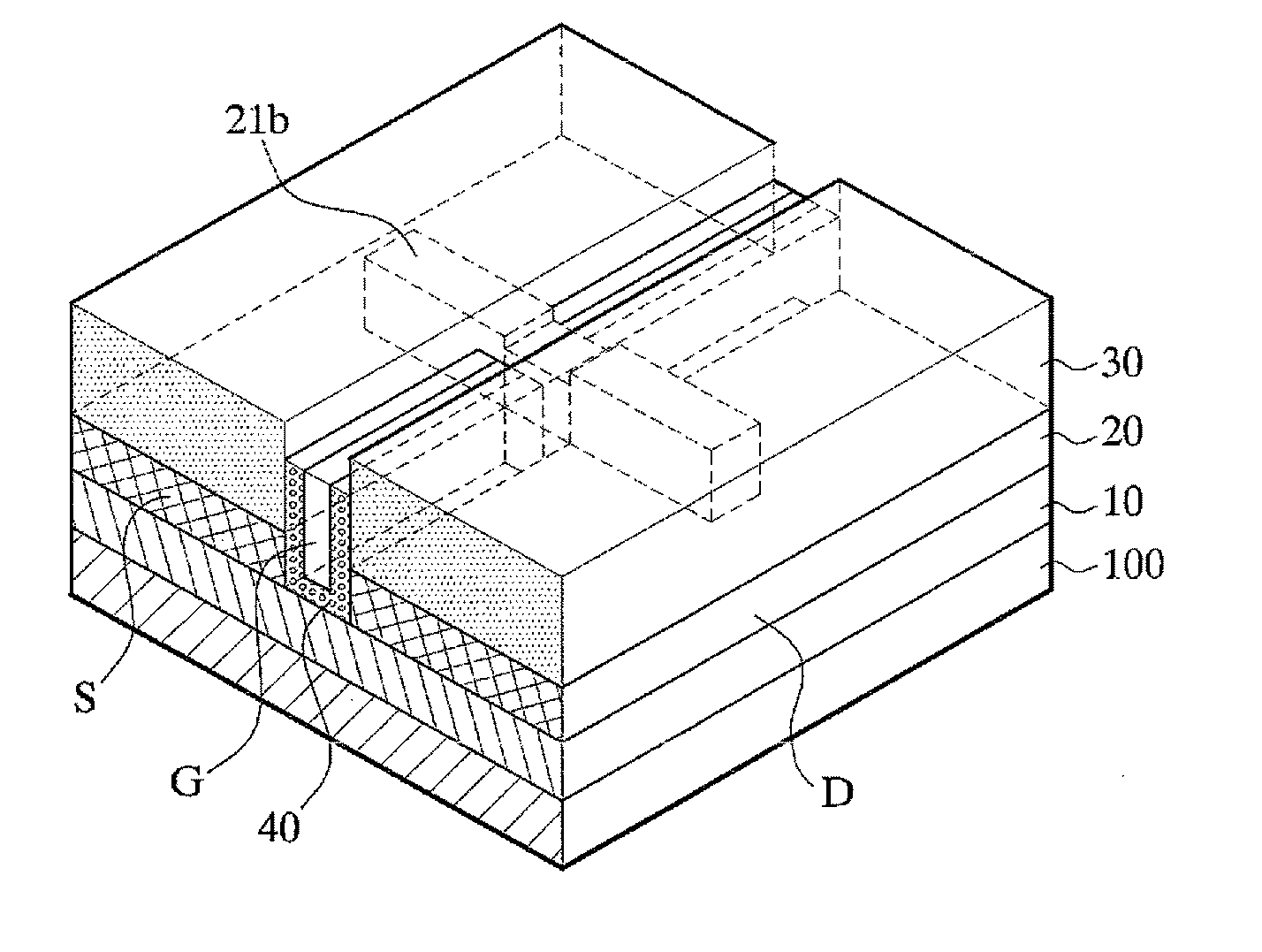
[0076]FIG. 22 is a cross-sectional perspective view showing a state in which a nano-wire structure 21b is formed according to a third embodiment of the present invention. A first step is a step of forming the nano-wire structure 21b. The nano-wire structure 21b is formed on a top silicon layer 20. In particular, the nano-wire structure 21b is formed by coating a resist on the top silicon layer 20, forming a pattern using a photolithography process or an electron-beam lithography process, and then etching the remaining portions other than the formed pattern. In a typical method, the nano-wire structure 21b is formed by depositing insulating material, forming a pattern using a lithography process, and then performing etching. In particular, the insulating material can include silicon oxide or silicon nitride. The nano-wire structure 21b is made of the insulating material.

[0077]FIG. 23 is a cross-sectional perspective view showing an example in which impurities ...


PUM


Abstract

The present invention relates to a single-electron transistor (SET) operating at room temperature and a method of manufacturing the same, and to be specific, to a single-electron transistor operating at room temperature and a method of manufacturing the same, which are capable of minimizing influence of the gate voltage on tunneling barriers and effectively controlling the electric potential of a quantum dot (QD), by forming the quantum dot using a trenched nano-wire structure and forming the gate to wrap most of the way around the quantum dot.

Description

CROSS REFERENCE TO RELATED APPLICATIONS[0001]This application is a continuation-in-part of U.S. patent application Ser. No. 12 / 866,886, filed on Aug. 9, 2010, and titled “Single Electron Transistor Operating at Room Temperature and Method Manufacturing for Same,” which is a National Phase Application under 35 U.S.C. §371 of International Application No. PCT / KR2009 / 000707 filed on Feb. 13, 2009, which claims priority from Republic of Korea Patent Application No. 10-2008-0014230 filed on Feb. 16, 2008, Republic of Korea Patent Application No. 10-2008-076550 filed on Aug. 5, 2008, and Republic of Korea Patent Application No. 10-2009-0010087 filed on Feb. 9, 2009, which are incorporated by reference herein in their entirety.BACKGROUND OF THE INVENTION[0002]1. Field of the Invention[0003]The present invention relates to a single-electron transistor (SET) operating at room temperature and a method of manufacturing the same, and to be specific, to a single-electron transistor operating at ...

Claims


Application Information

Patent Timeline
Patent Type & Authority Applications(United States)
IPC IPC(8): H01L21/335
CPCB82Y10/00H01L29/7613H01L29/66439Y10S438/962Y10S977/762Y10S977/937
Inventor CHOI, JUNG BUMSHIN, SEUNG JUN
Owner NANOCHIPS
Why Eureka
Try Eureka