Multi-component electronic package

a technology of integrated circuits and electronic packages, which is applied in the manufacture of printed circuits, basic electric elements, solid-state devices, etc., can solve the problems of compromising package performance, fragile final package form, and limited use of single-sided silicon substrates, so as to improve electrical performance and reduce the footprint , the effect of low profil

Active Publication Date: 2011-01-06
ATMEL CORP
View PDF30 Cites 17 Cited by
  • Summary
  • Abstract
  • Description
  • Claims
  • Application Information

AI Technical Summary

Benefits of technology

[0008]Package components are thus assembled onto the substrate to form an extremely compact, highly integrated, multi-component package or system-in-package (SIP) that provides an extremely small footprint and low profile. The electrical performance of the package is improved due to the ability to place the IC dice and other components in close proximity. The thin-film conductive interconnects formed on the planarized surfaces allow a much finer line width and spacing geometry in comparison with even the most advanced printed circuit board technologies. It also allows precise, high Q, integrated passive inductors to be formed in close proximity to the IC dice. With the interconnect layers deposited directly above and below the IC dice, a more efficient use is made of the package's footprint area, resulting in a smaller package size. The standard die-attach, wire bond or flip-chip attach processes can be eliminated by using this embedded components method.

Problems solved by technology

A silicon substrate can only be used in single-sided applications and is often fragile in the final package form.
The resultant longer interconnect lengths can also compromise package performance.

Method used


Image

  • Multi-component electronic package
  • Multi-component electronic package
  • Multi-component electronic package

Examples


Embodiment Construction

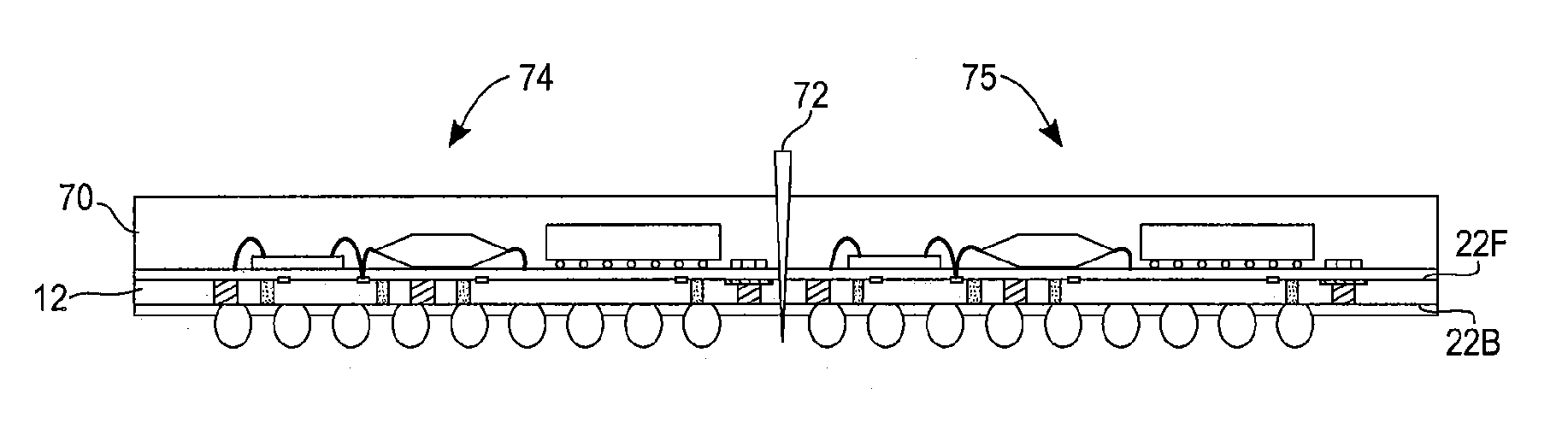
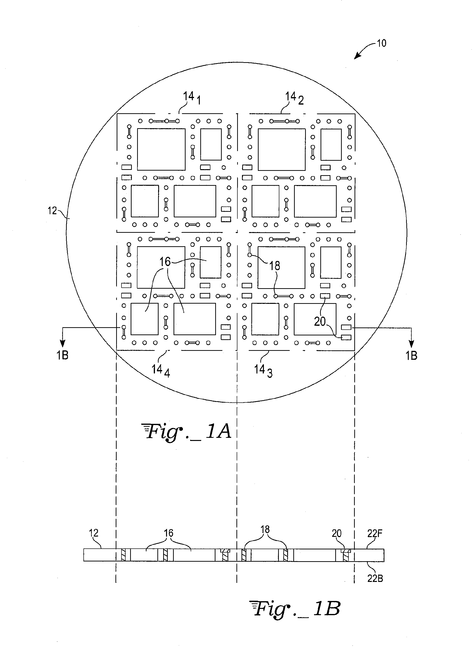
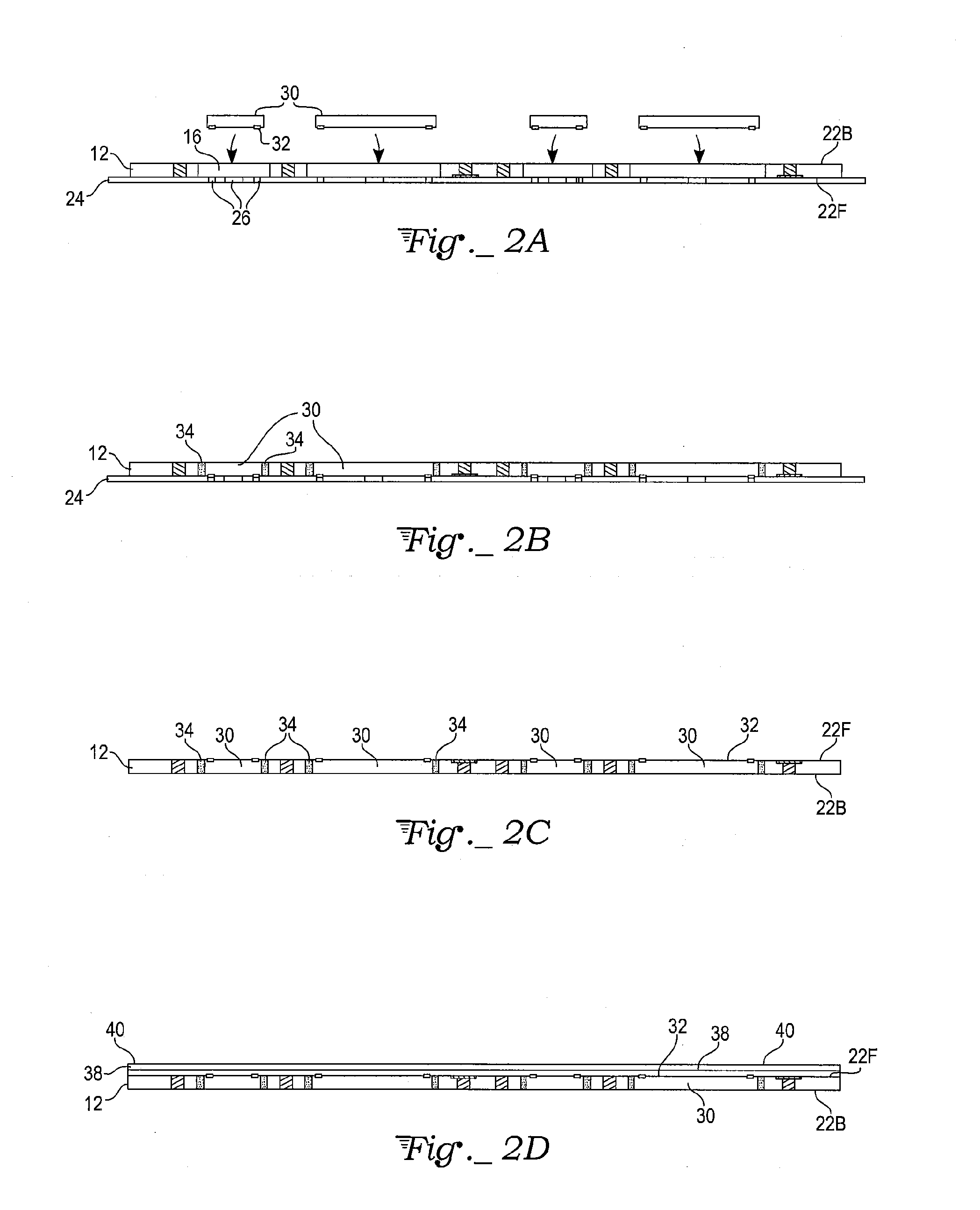
[0011]With reference to FIGS. 1A and 1B, a wafer 10 forms a substrate 12 for one or more IC chip packages. When cut into sections, e.g., 141, 142, 143, 144, each of those sections of the wafer 10 will define a separate package. The substrate 12 is typically composed of a dielectric material, such ceramics, glass, or plastics (e.g., epoxy, polyimide, or fluoropolymers). The substrate 12 has open cavities 16 into which IC die and other discrete electronic components will be placed. The width and length dimensions of the open cavities 16 are normally slightly larger than the components that will be inserted to allow tolerance for variations in the individual component size and room for adding an adhesive compound between the components and the inner periphery of the cavities 16.

[0012]Conductive vias 18 through the substrate 12 provide electrical pathways between the designated front and back surfaces 22F and 22B of the substrate 12 upon which electrical interconnects and other circuit ...


PUM

PropertyMeasurementUnit
conductiveaaaaaaaaaa
sizesaaaaaaaaaa
sizeaaaaaaaaaa

Abstract

An electronic multi-component package is assembled by placing multiple electronic components within multiple openings of a package substrate, then depositing and curing adhesive filler in gaps between the components and the inner peripheries of the openings. Circuit features, including conductive interconnects, are formed by thin-film photolithography over both front and back surfaces of the package substrate. Preformed conductive vias through the package substrate provide electrical connection between circuit features on opposite substrate surfaces. Additional electronic components may be attached to conductive lands on at least one side of the package. The circuit features also include contact pads for external package connections, such as in a ball-grid-array or equivalent structure.

Description

CLAIM OF PRIORITY[0001]This application is a continuation of and claims the benefit of priority under 35 U.S.C. §120 to U.S. patent application Ser. No. 11 / 557,864, entitled “MULTI-COMPONENT ELECTRONIC PACKAGE,” filed on Nov. 8, 2006, which is hereby incorporated by reference herein in its entirety.TECHNICAL FIELD[0002]The present invention relates to integrated circuit (IC) chip packages and the mounting of one or more IC dice to a support substrate and / or frame together with associated circuit components and interconnects.BACKGROUND ART[0003]Multi-component electronic packages and system-in-package (SIP) packages that are employed in the electronics industry today all utilize substrates for device inter-connection and attachment. Typical organic substrate materials are epoxy-glass, polyimide, and fluoropolymer laminates. Typical inorganic substrate materials are ceramics, low-temperature co-fire ceramics (LTCC) and silicon. The interconnect circuitry and component attach features ...

Claims


Application Information

Patent Timeline
Patent Type & Authority Applications(United States)
IPC IPC(8): H01L23/48H01L23/498H01L29/86
CPCH01L21/561Y10T29/49133H01L21/6835H01L23/5389H01L24/24H01L24/82H01L25/03H01L25/0652H01L25/16H01L2224/16227H01L2224/24011H01L2224/2518H01L2224/48091H01L2224/48227H01L2924/01013H01L2924/01027H01L2924/01058H01L2924/01078H01L2924/01082H01L2924/09701H01L2924/14H01L2924/19042H05K1/185H05K3/4602H05K2203/0165H05K2203/085H05K2203/1469H01L21/568Y10T29/53183Y10T29/49165Y10T29/4913H01L2224/97H01L2224/73267H01L24/97H01L24/96H01L24/48H01L2924/01005H01L2924/01006H01L2924/01023H01L2924/01033H01L2924/01076H01L2924/014H01L2224/16225H01L2224/0401H01L2224/04105H01L2924/00014H01L2224/81H01L2224/85H01L24/19H01L2924/181H01L2924/00012H01L2224/45099H01L2224/45015H01L2924/207
Inventor LAM, KEN M.
Owner ATMEL CORP
Why Eureka
Try Eureka