Ultra high density capacity comprising pillar-shaped capacitors formed on both sides of a substrate

Active Publication Date: 2011-01-06
NXP BV
View PDF19 Cites 14 Cited by
  • Summary
  • Abstract
  • Description
  • Claims
  • Application Information

AI Technical Summary

Benefits of technology

[0022]An advantage of the present invention is that the capacitors have a huge surface area. Another main advantage is the fact that, from a processing point of view, both sides of the wafer can be processed simultaneously.
[0023]The density of the capacitor obtained is typically larger than 70 nF/mm2, preferably larger than 150 nF/mm2, more preferably larger than 250 nF/mm2, even more preferably larger than 400 nF/mm2, such as larger than 600 nF/mm2 or even larger than 1 μF/mm2. As such, the present invention has increased, by more than a factor 2, the capacitance density values reached with in the prior art, e.g. with current PICS technology, by using both sides of the silicon wafer, and by making a via connection filled with the capacitance stack. The pillar like structure may have a circular form, an oval form, a rectangular form, such as a square form, a hexagonal form, an octagonal form, etc., or combinations thereof, preferably a circular form.
[0024]Typically the pillar like structure has a total diameter of 0.1-10 μm, preferably from 0.5-5 μm, more preferably from 0.8-3 μm, such as 2 μm. Clearly, the diameter and perimeter of a pillar structure are related by a factor π. Further, the pillar structure has a height of 30-900 μm, preferably from 50-600 μm, more preferably from 80-500 μm, such as 300 μm.
[0025]It is noted that a capacitor value is equal to ∈0∈rA/d. The pillar capacitor plays with its 3D-structure to incre

Problems solved by technology

These capacitance densities are for many applications not high enough.
Making narrower or deeper pillar structures is an option, but the increase in aspect ratio makes the structures more mechanically fragile and not attractive in terms of cost.
The use of other dielectric m

Method used


Image

  • Ultra high density capacity comprising pillar-shaped capacitors formed on both sides of a substrate
  • Ultra high density capacity comprising pillar-shaped capacitors formed on both sides of a substrate
  • Ultra high density capacity comprising pillar-shaped capacitors formed on both sides of a substrate

Examples


Embodiment Construction

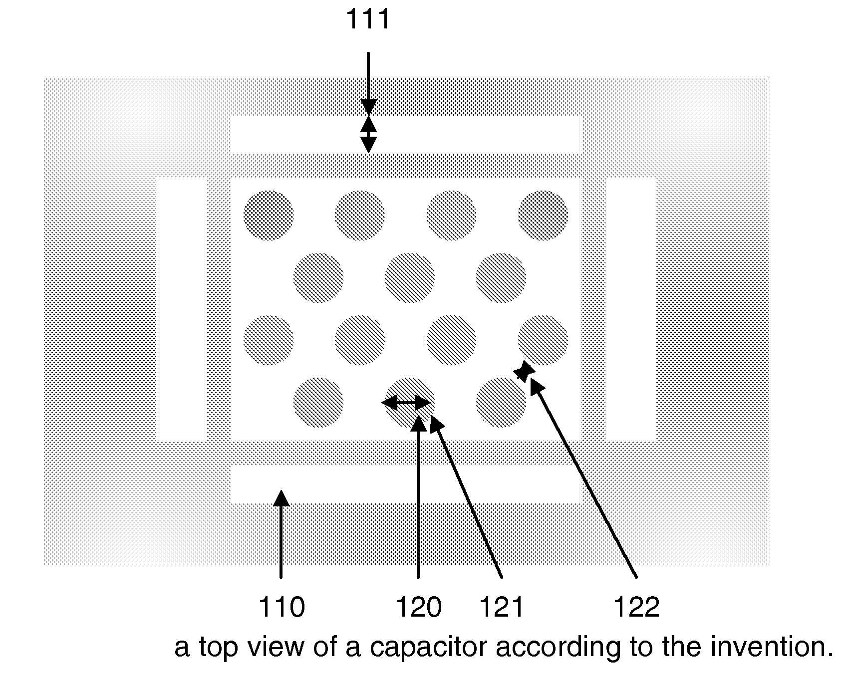
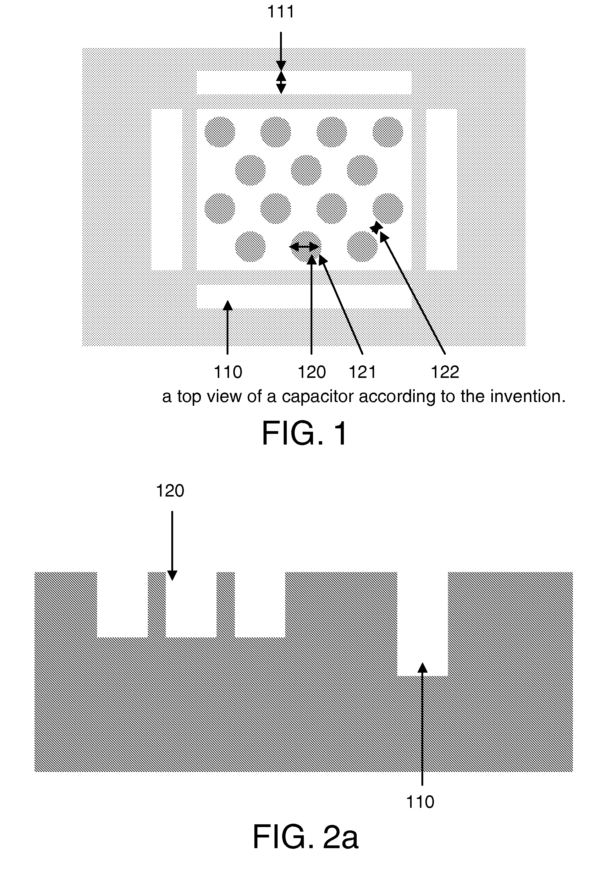
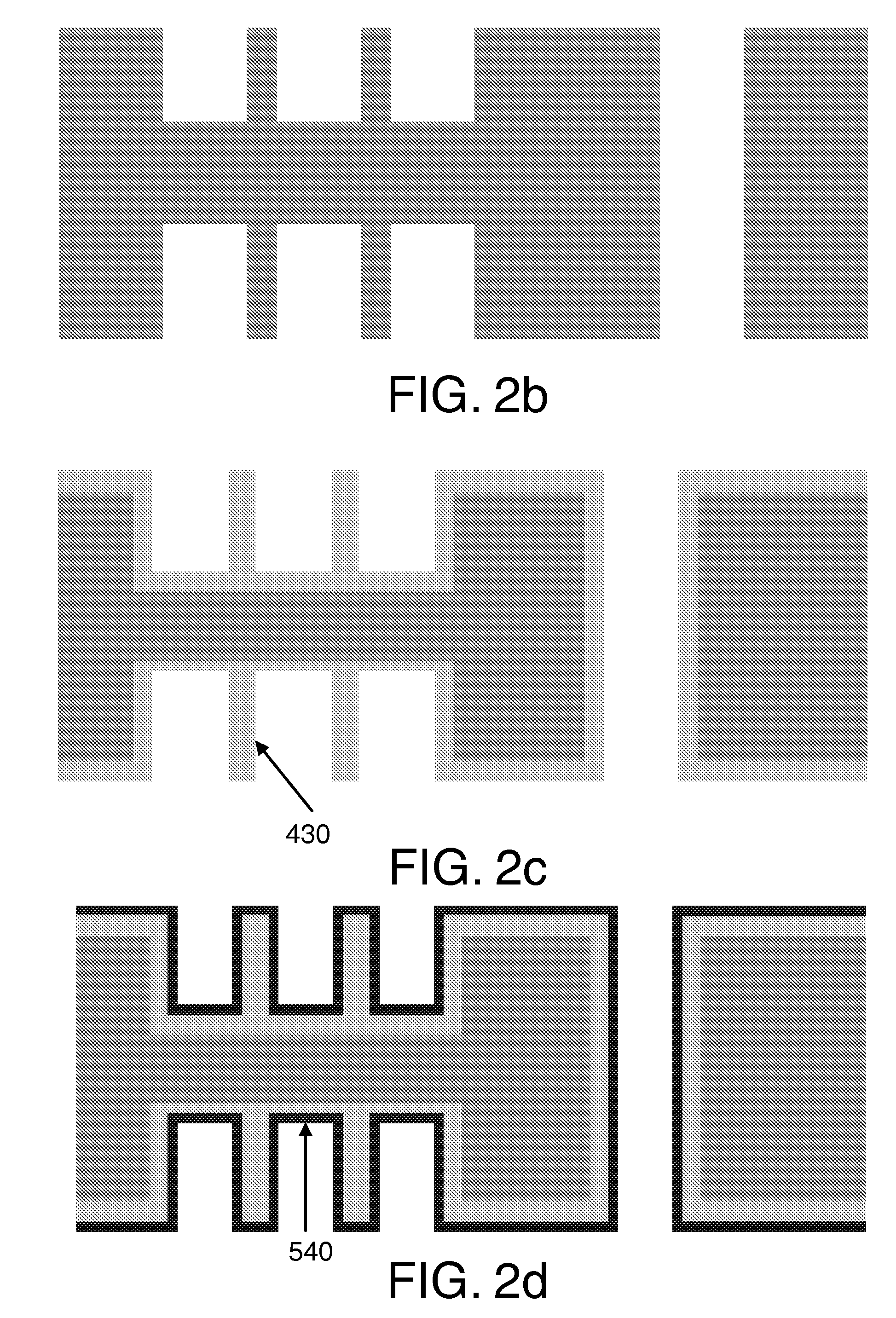
[0015]In a first aspect the invention relates to a semiconductor device with an ultra high density capacity, comprising a silicon substrate (900), more than one pillar like structure (910), preferably more than one pillar like structure on each side of the silicon substrate, at least one trench (920), preferably being a through substrate trench, a capacitor top electrode contact (981), and a capacitor bottom electrode contact (982), wherein the pillar structure comprises, seen from core to shaft, inner conductive material (950), dielectric material (940), and outer conductive material (930), preferably being doped silicon, wherein the trench comprises, seen from center to wall thereof, inner conductive material (950), preferably being poly silicon, dielectric material (940), and outer conductive material (930), preferably being doped silicon.

[0016]It is noted that the process could be asymmetric in nature. The pillars could in principle be on one side only, as an alternative to the ...


PUM


Abstract

The present invention describes an ultra High-Density Capacitor design, integrated in a semiconductor substrate, preferably a Si substrate, by using both wafer sides. The capacitors are pillar-shaped and comprise electrodes (930,950) separated by a dielectric layer (940). Via connections (920) are provided in trenches that go through the whole thickness of the wafer.

Description

FIELD OF THE INVENTION[0001]The present invention describes an ultra High-Density Capacitor design, integrated in a semiconductor substrate, preferably a Si substrate, preferably by using both wafer sides.BACKGROUND OF THE INVENTION[0002]High-Density Capacitors integrated in semiconductor substrates, especially on Si, are known in the art. They have been implemented mostly as trench (or pore) capacitors for applications as RF supply-line decoupling, phase-locked loop filtering and, even more abundantly, for trench capacitors for DRAM memories. Typical capacitance densities of capacitors obtained so far here are in the order of 25 nF / mm2, but are expected to increase to 70 nF / mm2 in the near future, which capacitors comprise a dielectric ONO layer, when reducing the ONO-based layer thickness to ˜15 nm. For DRAM applications the density is expressed in fF / μm2 and is—for logic technology reasons−comparable. These capacitance densities are for many applications not high enough. So there...

Claims


Application Information

Patent Timeline
IPC IPC(8): H01L29/92H01L21/02
CPCH01L23/49827H01L27/0207H01L27/0805H01L28/92H01L29/66181H01L2924/0002H01L29/945H01L2924/00H01L21/76898H01L23/481H01L2224/16145H01L23/642H01L2224/06181H01L2224/94H01L2224/03H01L2224/11
Inventor NEUILLY, FRANCOISLE CORNEC, FRANCOIS
Owner NXP BV
Why Eureka
Try Eureka