Multijunction photovoltaic cell grown on high-miscut-angle substrate

a photovoltaic cell and substrate technology, applied in the field of semiconductor materials, can solve the problems of increasing the cost of a launch more than linearly, increasing the cost of a launch, and the cost per watt of electrical power generation capacity of photovoltaic systems, and achieves the effects of high band gap, quantum efficiency, and short cutoff wavelength

Inactive Publication Date: 2011-01-20
THE BOEING CO
View PDF11 Cites 72 Cited by
  • Summary
  • Abstract
  • Description
  • Claims
  • Application Information

AI Technical Summary

Benefits of technology

[0026]In another aspect of the present invention, a method for producing a shorter cutoff wavelength for the external quantum efficiency of a GaInP top subcell comprises providing a Ge substrate with a 15.8 degree miscut angle, and growing the disordered GaInP top subcell on the 15.8°-miscut Ge substrate, resulting in a high bandgap and a quantum efficiency percentage of about zero by a wavelength of about 675 nm.
[0027]In a further aspect of the present invention, a method for increasing a conversion efficiency in a solar cell comprises providing a Ge substrate with a 15.8 degree miscut angle, and growing a GaInP top subcell on the 15.8°-miscut Ge substrate, resulting in an conversion efficiency under the AM0 spectrum of about 28% or higher and an open-circuit voltage of about 2.7 V.

Problems solved by technology

The interest in PV cells or solar cells has been increasing due to concerns regarding pollution and limited available resources.
Increasing the payload of a spacecraft in this manner increases the cost of a launch more than linearly.
The cost per watt of electrical power generation capacity of photovoltaic systems may be a main factor, which inhibits their widespread use in terrestrial applications.
Addition of even small amounts of aluminum to the top cell to form AlInGaP simultaneously incorporates oxygen and thus quickly degrades the minority-carrier lifetime and performance of the device.
If the currents are different, the subcell with the lowest photogenerated current will limit the current through all of the series-interconnected subcells in the multijunction (MJ) cell, and excess photogenerated current in other subcells is wasted.
Limiting the current in this manner results in a severe penalty on the MJ cell efficiency.
For the multiple-cell PV device, efficiency may be limited by the requirement of low resistance interfaces between the individual cells to enable the generated current to flow from one cell to the next.
In addition to providing the lowest resistance path possible between adjacent subcells, the tunnel junction should also be transparent to wavelengths of light that can be used by lower subcells in the MJ stack, because of the poor collection efficiency of carriers photogenerated in the tunnel junction region.
Such Zn doping and diffusion, however, alters the material properties of the GaInP top subcell (and potentially other subcells and layers) resulting in non-ideal output and efficiency of the PV cell.
A limitation of such a conventional method includes incomplete disordering of the GaInP group-III sublattice, resulting in a lower bandgap and cell voltage than possible with a more complete disordering.
In addition, the top subcell device parameters and manufacturability of the MJ cell can be negatively impacted by the requirement to have a high Zn concentration in all or part of the base of the GaInP top subcell.
In such situations, the disordering of the GaInP top subcell remains incomplete unless rather extreme growth conditions are used, thus placing constraints on the MJ cell growth process that are adverse to the cell's output and efficiency.
For example, high growth temperature can degrade the performance of other subcells in the MJ stack, and high growth rates can impose inconveniently high levels of group-III source flows during growth.

Method used


Image

  • Multijunction photovoltaic cell grown on high-miscut-angle substrate
  • Multijunction photovoltaic cell grown on high-miscut-angle substrate
  • Multijunction photovoltaic cell grown on high-miscut-angle substrate

Examples


Embodiment Construction

[0035]The following detailed description describes the best currently contemplated modes of carrying out the invention. The description should not be taken in a limiting sense, but is made merely for the purpose of illustrating the general principles of the invention, since the scope of the invention is best defined by the appended claims.

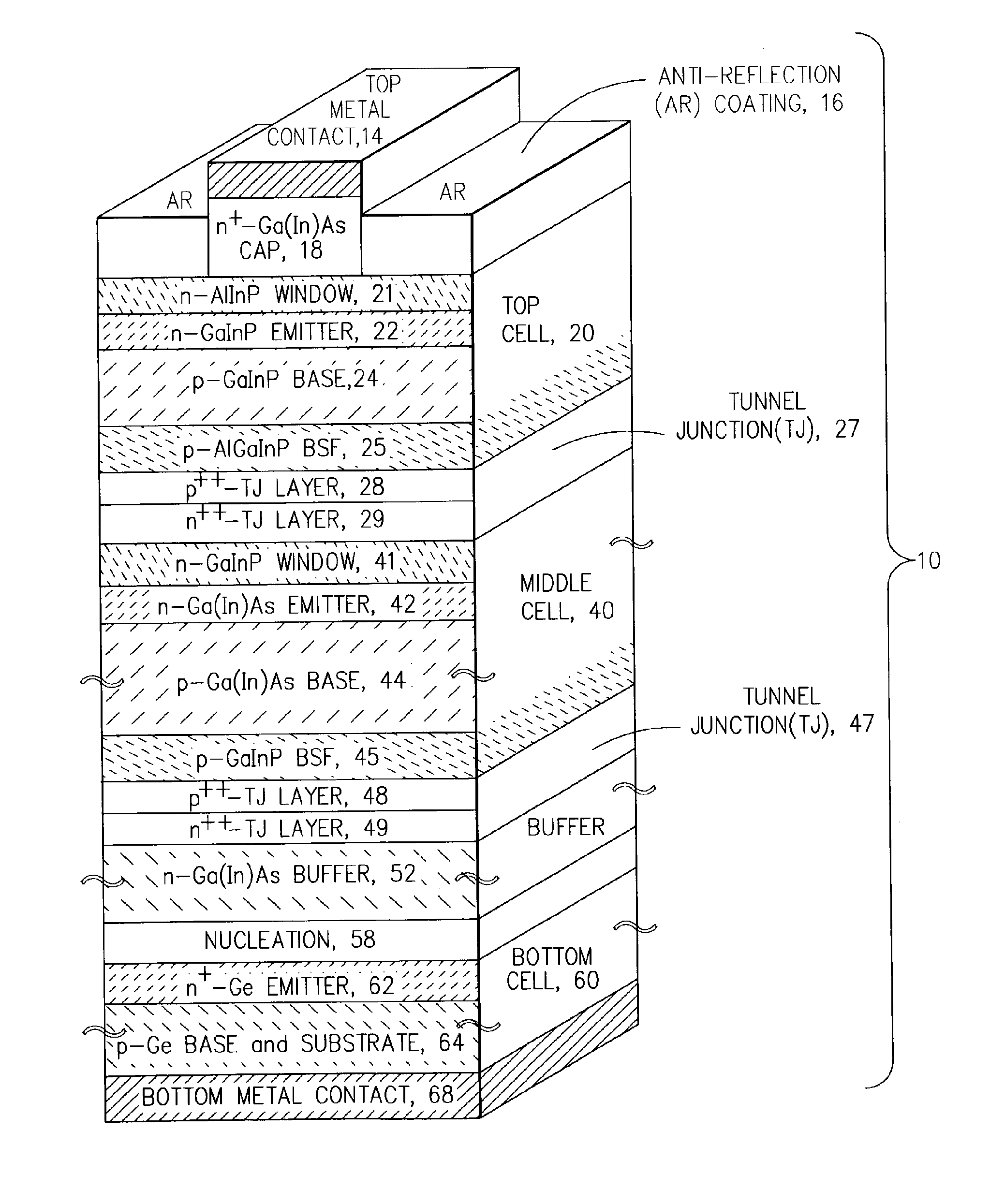
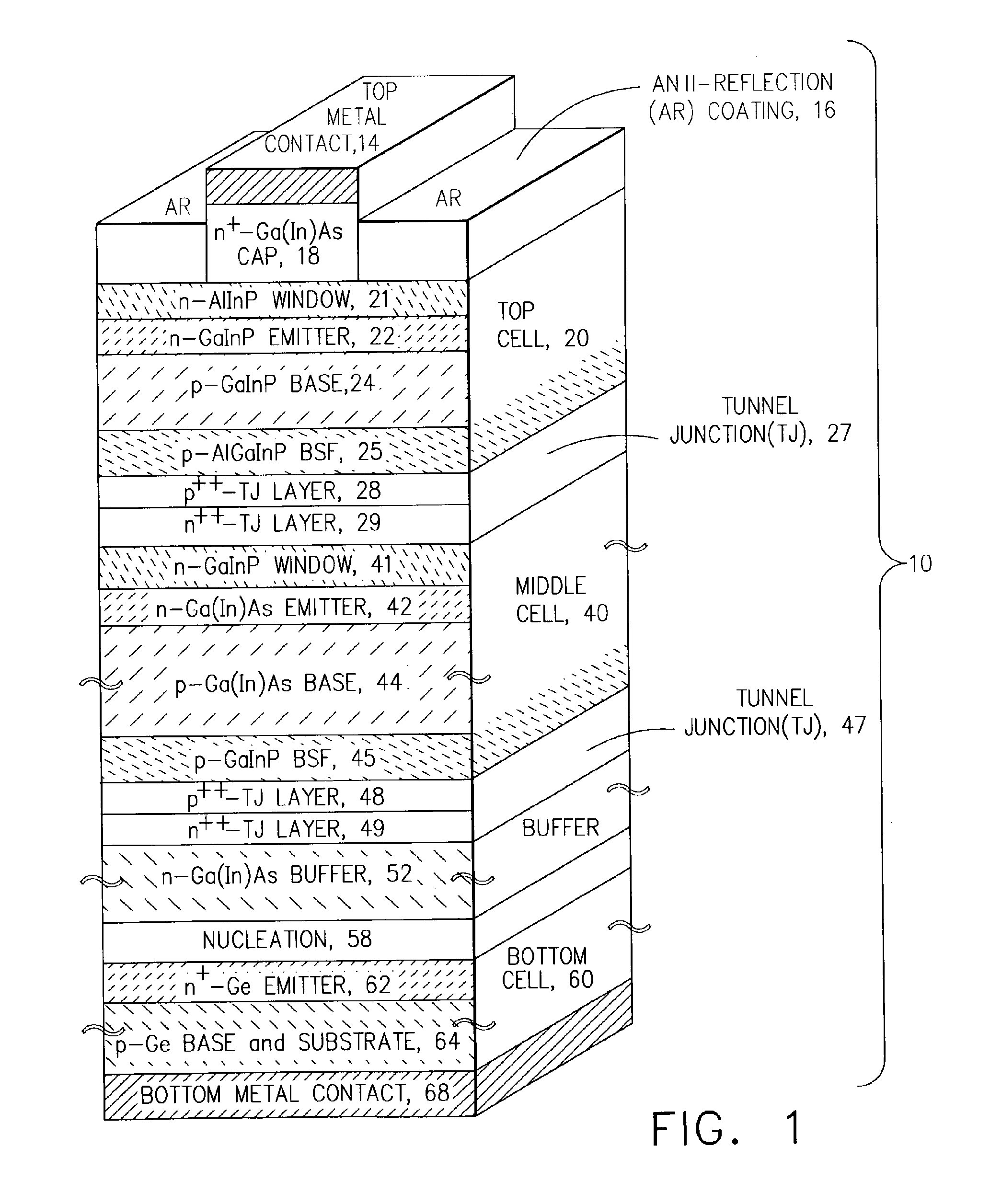
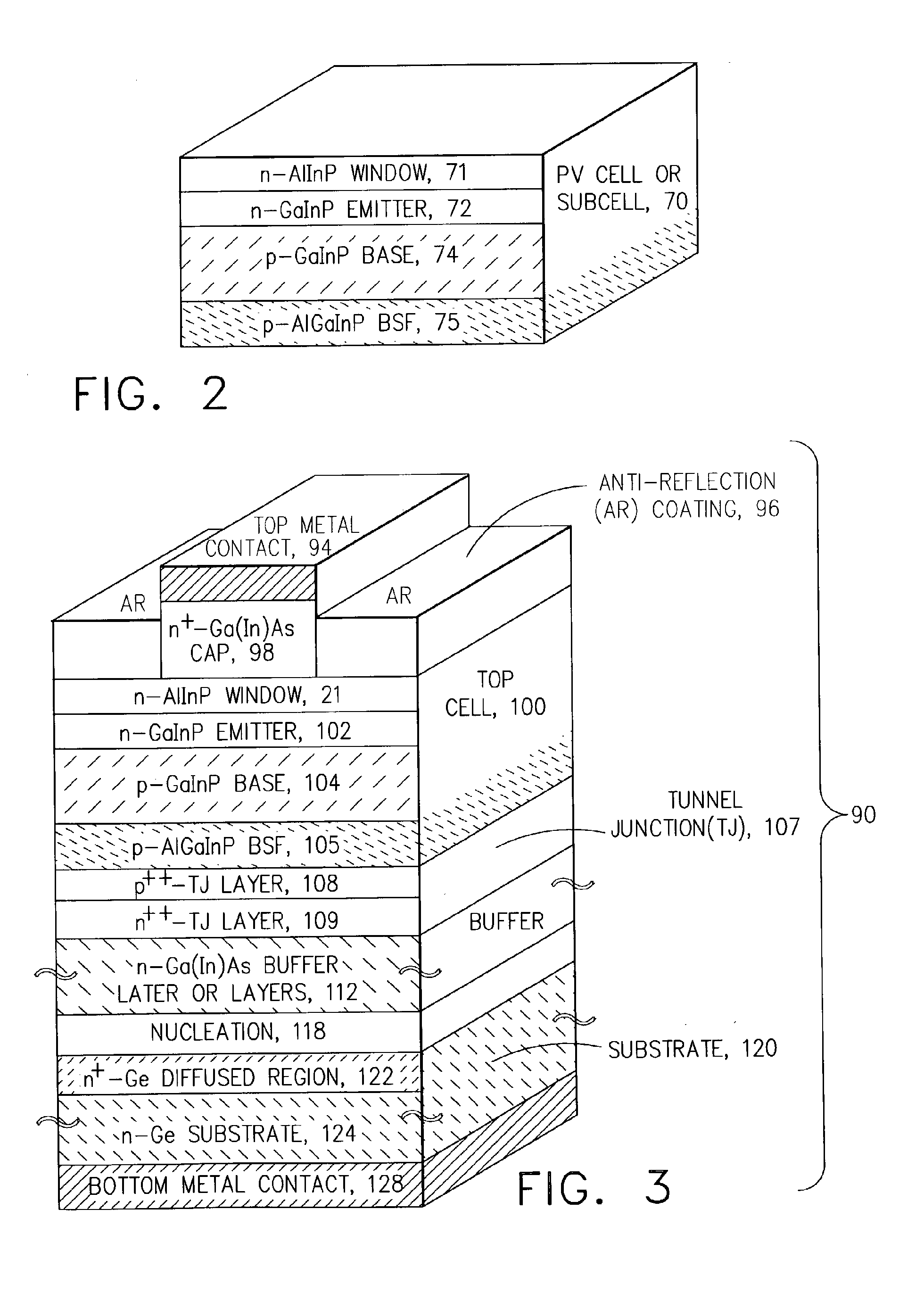
[0036]The present invention generally provides a high-efficiency MJ photovoltaic cell (such as a GaInP / Ga(In)As / Ge cell) that may be used with, for example, a satellite. Such a high-efficiency MJ photovoltaic cell results from an increased bandgap of the GaInP subcell, due to an increased sublattice disorder induced by growth on a substrate misoriented from a (100) plane toward a (111) plane. Any of the aforementioned conventional methods for disordering GaInP (and other III-V compounds) can be used in conjunction with disordering due to growth on high-miscut-angle substrates of the present invention.

[0037]Referring now to FIG. 1, a cross-section o...


PUM


Abstract

The present invention provides a photovoltaic cell comprising a GaInP subcell comprising a disordered group-III sublattice, a Ga(In)As subcell disposed below the GaInP subcell, and a Ge substrate disposed below the Ga(In)As subcell comprising a surface misoriented from a (100) plane by an angle from about 8 degrees to about 40 degrees toward a nearest (111) plane.

Description

GOVERNMENT INTERESTS[0001]The United States Government has rights in this invention under Contract No. F29601-98-2-0207 between The Boeing Company and the U.S. Air Force.BACKGROUND OF THE INVENTION[0002]The present invention generally relates to semiconductor materials and, more specifically, to photovoltaic (PV) cells and optoelectronic devices grown on high-miscut-angle substrates.[0003]The interest in PV cells or solar cells has been increasing due to concerns regarding pollution and limited available resources. This interest has been in both terrestrial and non-terrestrial applications. In space applications, the use of nuclear or battery power greatly increases a spacecraft's payload for a given amount of required power to operate the satellite. Increasing the payload of a spacecraft in this manner increases the cost of a launch more than linearly. With the ready availability of solar energy in outer space for a spacecraft such as a satellite, the conversion of solar energy int...

Claims


Application Information

Patent Timeline
Patent Type & Authority Applications(United States)
IPC IPC(8): B64G1/44H01L31/0256H01L31/042H01L31/18H01L21/20H01L31/04H01L31/00H01L31/0687
CPCH01L31/036H01L31/0687Y02E10/544H01L31/1852Y02E10/52H01L31/1844Y02E10/547Y02P70/50
Inventor KING, RICHARD R.ERMER, JAMES H.COLLER, PETER C.FETZER, CHRIS
Owner THE BOEING CO
Why Eureka
Try Eureka