Semiconductor light-emitting device and method for manufacturing the same

a technology manufacturing methods, which is applied in the direction of semiconductor/solid-state device manufacturing, semiconductor devices, electrical equipment, etc., can solve the problems of inevitable increase in the manufacturing cost of semiconductor light-emitting devices, achieve high conductivity, and achieve high optical reflectance.

Inactive Publication Date: 2011-01-20
SONY CORP
View PDF2 Cites 16 Cited by
  • Summary
  • Abstract
  • Description
  • Claims
  • Application Information

AI Technical Summary

Benefits of technology

[0036]In the present invention, since the second electrode is composed of a titanium oxide having a high electron density, not only high conductivity can be achieved, but also high optical reflectance can be achieved. As a result, the emission efficiency of the semiconductor light-emitting device can be significantly improved. In addition, since the second electrode is composed of a titanium oxide, a problem

Problems solved by technology

However, the second electrode composed of such a metal easily causes electrical migration in a process for manufacturing a semiconductor light-emitting device or during an operation of a semico

Method used


Image

  • Semiconductor light-emitting device and method for manufacturing the same
  • Semiconductor light-emitting device and method for manufacturing the same
  • Semiconductor light-emitting device and method for manufacturing the same

Examples


embodiment 1

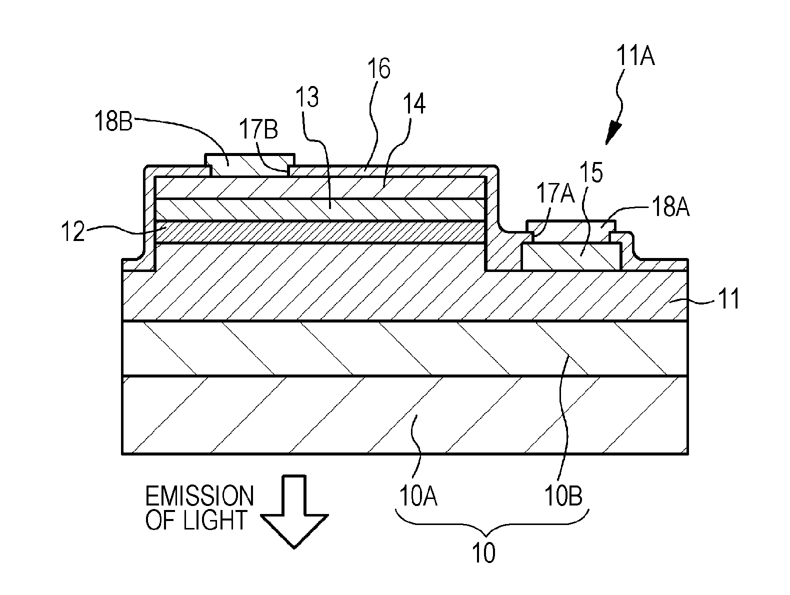
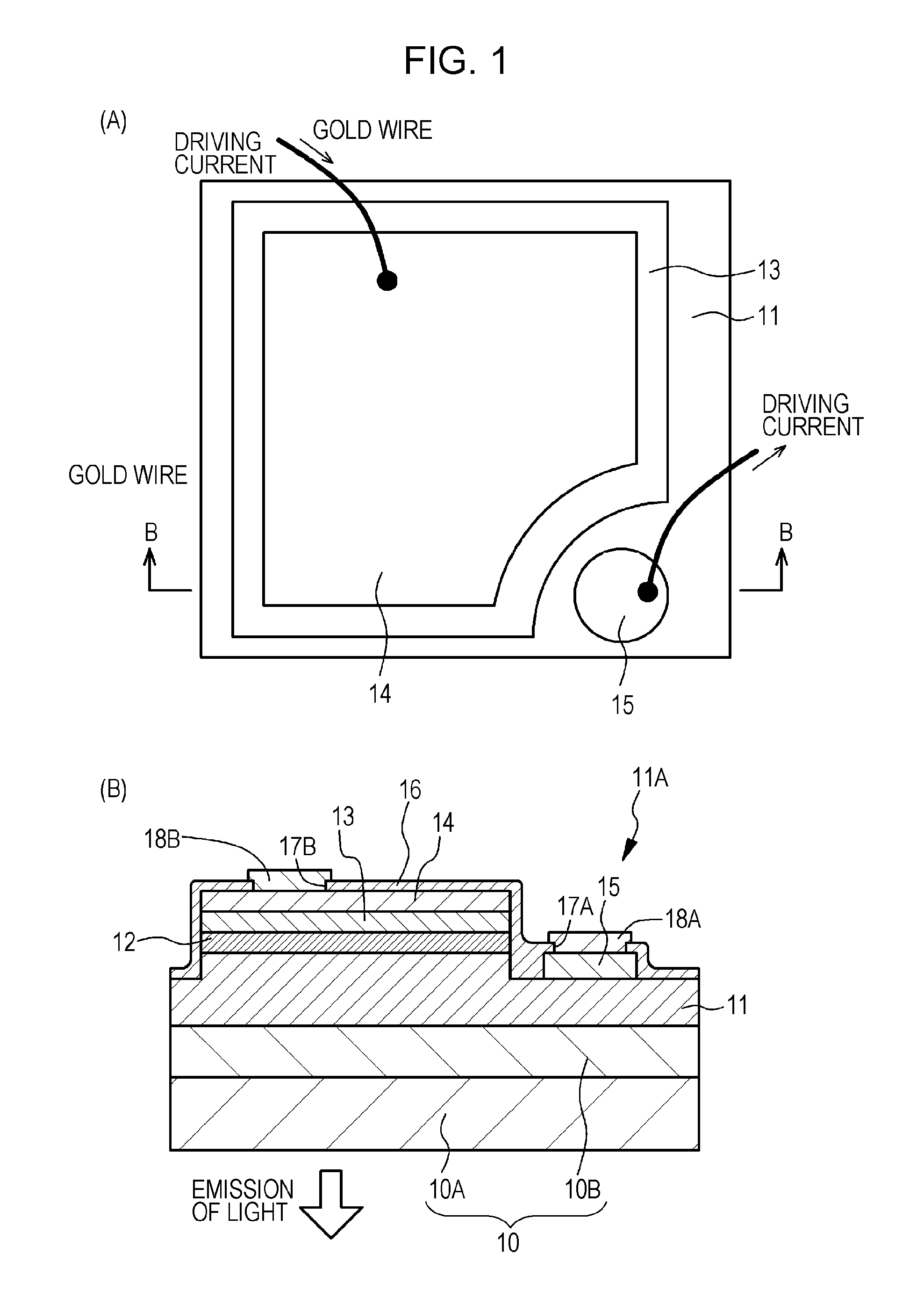
[0050]Embodiment 1 relates to a semiconductor light-emitting device of the present invention and a method for manufacturing the same.

[0051]A semiconductor light-emitting device of Embodiment 1 includes a light-emitting diode (LED), and as shown in FIG. 1(A) which is a schematic layout drawing of components and FIG. 1(B) which is a schematic sectional view taken along arrow B-B in FIG. 1(A), is provided with:

[0052](A) a first compound semiconductor layer 11 having an n-type conductivity type;

[0053](B) an active layer 12 formed on the first compound semiconductor layer 11 and composed of a compound semiconductor;

[0054](C) a second compound semiconductor layer 13 formed on the active layer 12 and having a p-type conductivity type;

[0055](D) a first electrode 15 electrically connected to the first compound semiconductor layer 11; and

[0056](E) a second electrode 14 formed on the second compound semiconductor layer 13.

[0057]In addition, the second electrode 14 is composed of a titanium oxi...


PUM


Abstract

There is provided a light-emitting device including a second electrode which exhibits a stable behavior in a process for manufacturing a light-emitting device or during an operation of a light-emitting device. A light-emitting device includes a first compound semiconductor layer 11 with an n-type conductivity type, an active layer 12 formed on the first compound semiconductor layer 11 and composed of a compound semiconductor, a second compound semiconductor layer 13 with a p-type conductivity type formed on the active layer 12, a first electrode 15 electrically connected to the first compound semiconductor layer 11, and a second electrode 14 formed on the second compound semiconductor layer 13, wherein the second electrode 14 is composed of a titanium oxide, has an electron concentration of 4×10²¹/cm3 or more, and reflects light emitted from the active layer.

Description

TECHNICAL FIELD[0001]The present invention relates to a semiconductor light-emitting device and a method for manufacturing the same.BACKGROUND ART[0002]Semiconductor light-emitting devices such as light-emitting diodes (LED) and the like have, for example, a structure in which a first compound semiconductor layer 11 with an n-type conductivity type, an active layer 12, and a second compound semiconductor layer 13 with a p-type conductivity type are laminated in order on a substrate 10. In addition, a first electrode (n-side electrode) 15 is provided on the substrate or an exposed portion 11A of the first compound semiconductor layer 11, and a second electrode (p-side electrode) 114 is provided on the top of the second compound semiconductor layer 13. Such semiconductor light-emitting devices can be classified into the two types including a type of semiconductor light-emitting device in which light from the active layer 12 is emitted through the second compound semiconductor layer 13...

Claims


Application Information

Patent Timeline
IPC IPC(8): H01L33/30H01L33/00H01L21/28H01L33/06H01L33/10H01L33/32H01L33/36H01L33/40
CPCH01L33/007H01L33/32H01L33/44H01L33/405H01L33/40
Inventor HITSUDA, YUKIHISAOHASHI, TATSUO
Owner SONY CORP
Why Eureka
Try Eureka