Method of fabricating transistors and a transistor structure for improving short channel effect and drain induced barrier lowering

a technology of short channel effect and transistor structure, which is applied in the direction of transistors, semiconductor devices, electrical appliances, etc., can solve the problems of reducing the efficiency of transistors, reducing the electron mobility of mos transistors, and reducing the driving current of mos transistors, so as to improve the short channel effect and the effect of drain induced barrier lowering

Active Publication Date: 2011-01-20
UNITED MICROELECTRONICS CORP
View PDF3 Cites 21 Cited by
  • Summary
  • Abstract
  • Description
  • Claims
  • Application Information

AI Technical Summary

Benefits of technology

[0010]According to the present invention, a transistor structure for improving short channel effect and drain induced barrier lowering comprises: a substrate comprising a P-type well; a gate disposed on the P-type well; a spacer disposed on the gate; a N-type source / drain region disposed in the substrate at two sides of the gate; a silicon cap layer covering the N-type source / drain region; and a silicide layer disposed on the silicon cap.
[0011]The feature of the present invention is that, after forming the epitaxial layer, a silicon cap layer is formed at two sides of the gate of NMOS and PMOS respectively. In other words, the silicon cap layer is formed on the surface of the source / drain region of the NMOS and PMOS. The silicon cap layer can level up the baseline of the source / drain region of the NMOS after the mask is removed. In this way, the short channel effect and the drain induced barrier lowering effect can be prevented because the depth of the p / n junction is maintained at a predetermined depth. Furthermore, the epitaxial layer will become a spacer of the NMOS after the epitaxial layer is formed.

Problems solved by technology

As the semiconductor processes advance to the very deep sub micron era such as 65-nm node or beyond, how to increase the driving current for MOS transistors has become a critical issue.
An SiGe layer deposited into the predetermined source / drain region often increases the mobility of electron holes of PMOS, but will simultaneously decrease the electron mobility of an NMOS and reduce the efficiency of the transistor.
However, the surface of the substrate where the predetermined source / drain region of NMOS is disposed will be corroded by hot phosphoric acid.

Method used


Image

  • Method of fabricating transistors and a transistor structure for improving short channel effect and drain induced barrier lowering
  • Method of fabricating transistors and a transistor structure for improving short channel effect and drain induced barrier lowering
  • Method of fabricating transistors and a transistor structure for improving short channel effect and drain induced barrier lowering

Examples


Embodiment Construction

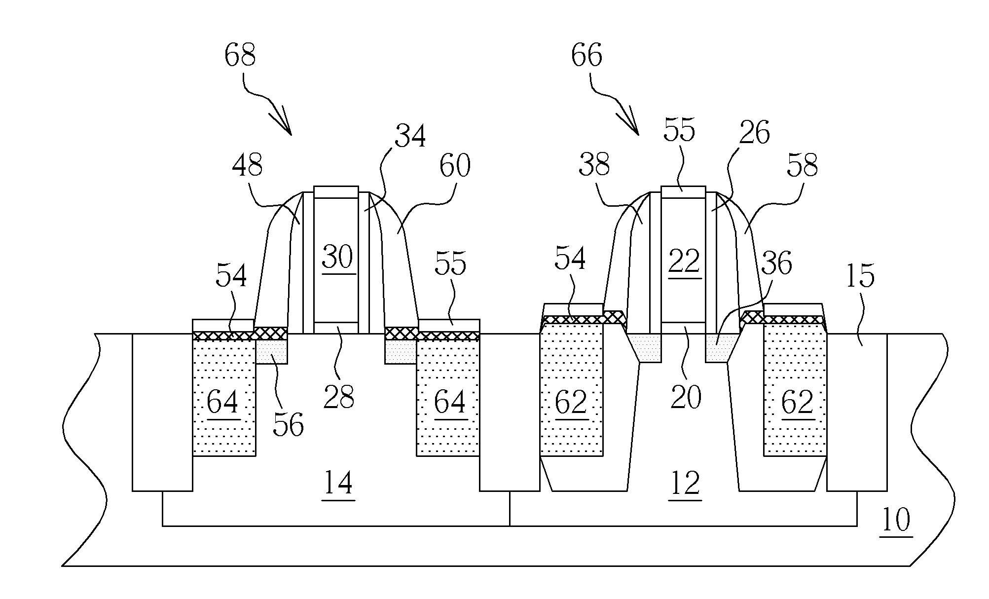
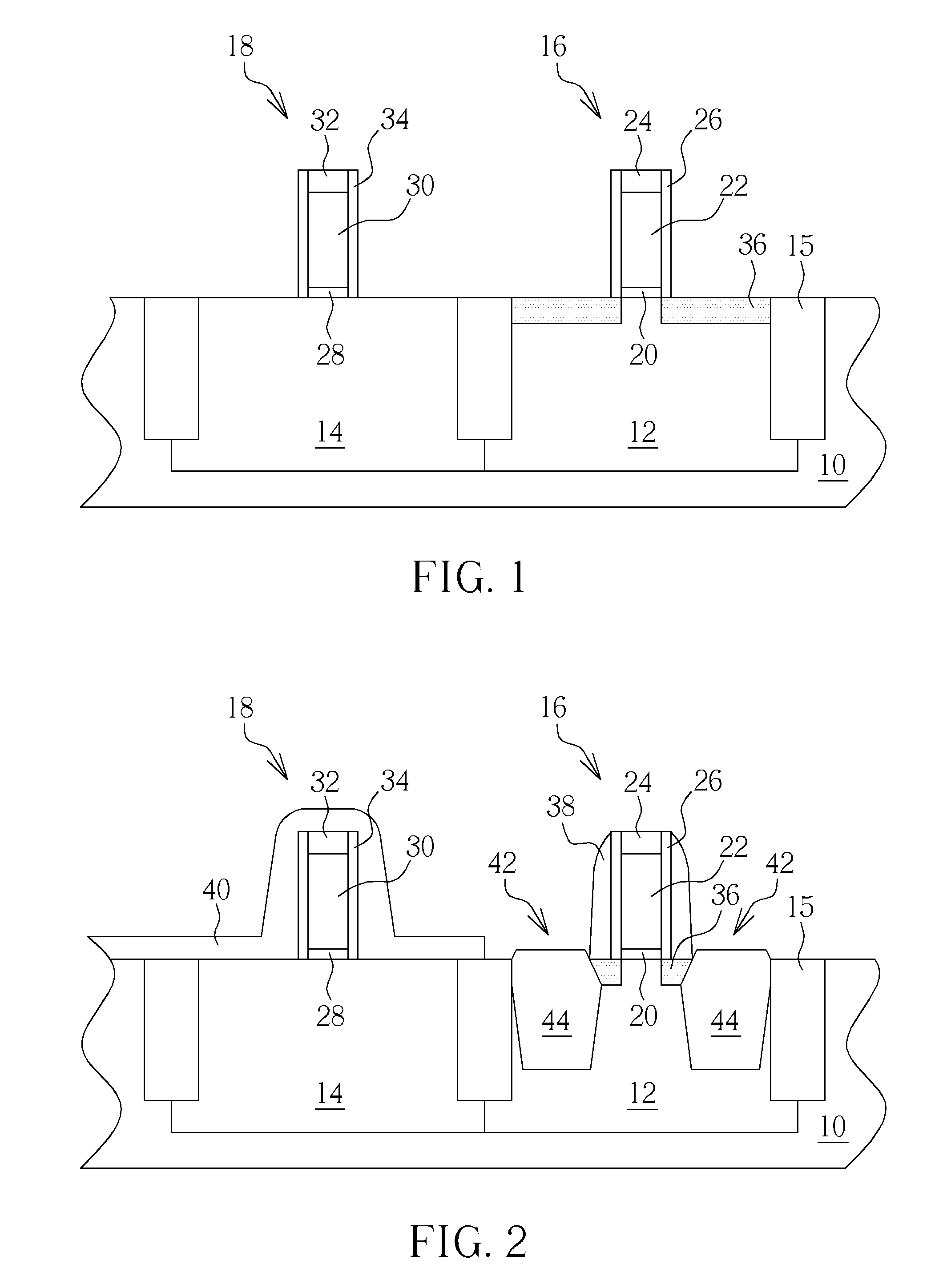
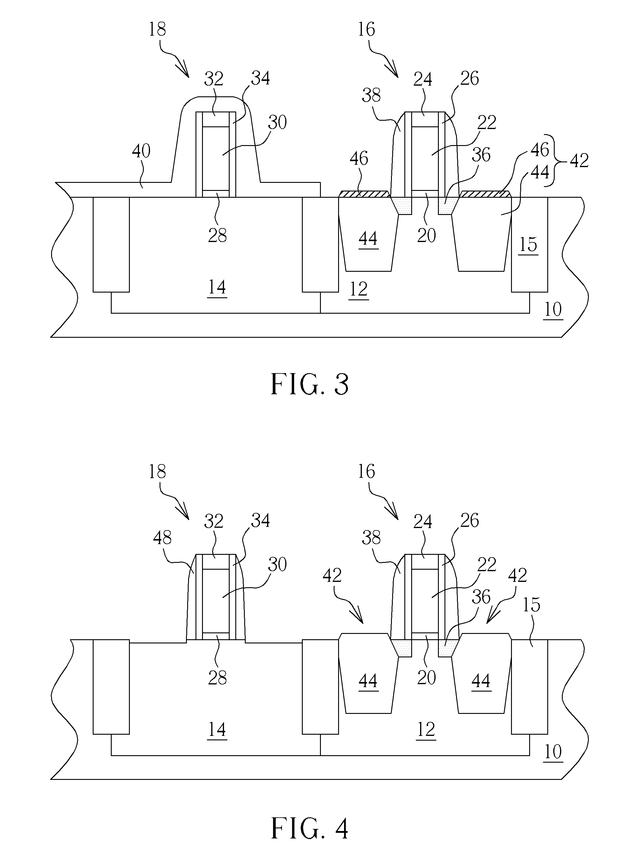
[0015]FIG. 1 through FIG. 9 are schematic cross-section view diagrams showing the means of fabricating transistors according to the present invention.

[0016]As shown in FIG. 1, first, a substrate 10 comprising a first type well 12 and a second type well 14 are provided. The first type well 12 may be an N type or P type, and the second type well 14 may be a P type or N type. The following illustration will take the first type well 12 as an N type well, and the second type well 14 as a P type well. In other words, a PMOS will be formed on the first type well 12 and a NMOS will be formed on the second type well 14. In addition, a shallow trench isolation (STI) 15 is disposed between the first type well 12 and the second type well 14, and around the first type well 12 and the second type well 14 within the semiconductor substrate 10.

[0017]Next, a first gate 16 and a second gate 18 are formed on the first type well 12 and the second type well 14, respectively. The first gate 16 includes a...


PUM


Abstract

A method of fabricating transistors includes: providing a substrate including an N-type well and P-type well; forming a first gate on the N-type well and a second gate on the P-type well, respectively; forming a third spacer on the first gate; forming an epitaxial layer in the substrate at two sides of the first gate; forming a fourth spacer on the second gate; forming a silicon cap layer covering the surface of the epitaxial layer and the surface of the substrate at two sides of the fourth spacer; and forming a first source/drain doping region and a second source/drain doping region at two sides of the first gate and the second gate respectively.

Description

BACKGROUND OF THE INVENTION [0001]1. Field of the Invention[0002]The present invention relates to a method of manufacturing a semiconductor device, and a semiconductor structure thereof for improving short channel effect and drain induced barrier lowering, and more particularly, to a method of manufacturing MOS transistors, and a MOS structure thereof that improves short channel effect and drain induced barrier lowering.[0003]2. Description of the Prior Art[0004]For decades, chip manufacturers have made metal-oxide-semiconductor (MOS) transistors faster by making them smaller. As the semiconductor processes advance to the very deep sub micron era such as 65-nm node or beyond, how to increase the driving current for MOS transistors has become a critical issue.[0005]To attain higher performance of a semiconductor device, attempts have been made to use a strained silicon (Si) layer for increasing the mobility of electrons or holes. For example, taking advantage of the lattice constant ...

Claims


Application Information

Patent Timeline
Patent Type & Authority Applications(United States)
IPC IPC(8): H01L29/78H01L21/8234
CPCH01L21/823807H01L21/823814H01L29/665H01L27/092H01L29/66628H01L29/7848H01L29/6656
Inventor HUNG, WEN-HANCHEN, TSAI-FUTING, SHYH-FANNHUANG, CHENG-TUNGLEE, KUN-HSIENLO, TA-KANGCHENG, TZYY-MING
Owner UNITED MICROELECTRONICS CORP
Why Eureka
Try Eureka