Method for Strengthening Adhesion Between Dielectric Layers Formed Adjacent to Metal Layers

a dielectric layer and metal layer technology, applied in the field of microelectronic processing, can solve the problems of poor catalytic activity, poor quality metal deposits, exposure of the substrate surface to air during the transfer, etc., and achieve the effects of reducing material and waste disposal costs, preventing oxidation, and reducing the oxidation of the topography

Inactive Publication Date: 2011-01-20
LAM RES CORP
View PDF59 Cites 11 Cited by
  • Summary
  • Abstract
  • Description
  • Claims
  • Application Information

AI Technical Summary

Benefits of technology

[0021]In either case, the process chamber may further include a gate latch configured to align barriers of the gate latch with the wall opening and the gate casing opening. In some embodiments, the gate latch is configured to move within the space between the wall and gate casing. In this manner, the gate latch may be configured to move the barriers such that the barriers are not in alignment with the wall opening and gate casing opening as well. In some cases, the portion of the gate latch comprising the barriers may be configured to move such that the two openings are either sealed or provide an air passage to the process chamber when the barriers are respectively aligned with the two openings. In this manner, the barriers may prevent fluids within the process chamber from flowing through the wall opening and gate casing opening whenever the barriers are respectively aligned with the two openings. In some embodiments, the process chamber may be adapted to draw air through the air passage and into the process chamber.
[0041]Furthermore, the method which deposits a hydrophobic layer upon dielectric portion of the topography prior to the deposition of a cap layer may advantageously prevent the deposition of a the layer upon dielectric portions of a topography, potentially preventing the formation of a short within the device.

Problems solved by technology

Another common problem with treating a surface in a series of baths is the exposure of the substrate surface to air during the transfer between baths.
Such an exposure to air may cause oxidation of the substrate surface that will result in poor catalytic activity and poor quality metal deposits.
This problem becomes especially troublesome when using materials that easily oxidize in air, such as copper.
Such apparatuses, however, fail to prevent the solutions from the plurality of different process steps from mixing once they are expelled from the process chamber.
Consequently, the apparatuses may not reuse process solutions within the apparatus, incurring higher material costs and waste disposal costs for the electroless deposition process.
In addition, such apparatuses fail to provide a manner with which to supply air exterior to the process chamber during processing, such as for a drying step, for example.
In particular, prior art apparatuses may only offer two modes of operation, one in which the chamber is sealed for processing and another in which the chamber is not sealed for loading.
In other cases, prior art apparatuses may not be sealed at all.
In any embodiment, another problem with conventional process chambers is the manner in which a substrate is secured within the process chamber.
In particular, few conventional process chambers offer a manner with which to secure a substrate without causing damage to the substrate, particularly along the edges of the substrate.
One common drawback of existing electroless deposition processes and apparatuses is low speed of deposition.
However, many electroless deposition solutions tend to decompose at high temperatures, leading to significant non-uniformities in the deposited material.
On the other hand, deposition rates of electroless solutions at relatively low temperatures may be undesirably low, reducing production throughput and increasing fabrication costs.
Another common problem with electroless deposition processes is the formation of gas bubbles on the substrate surface during processing.
The gas bubbles undesirably prevent a material from being deposited uniformly upon a substrate surface, potentially depositing a layer outside the specifications of the process.
In some cases, however, it may be difficult to clean and activate the barrier layer for a sufficient deposition of a bulk metal layer.
In particular, the barrier layer may be cleaned and activated for the deposition of the bulk metal layer, but it may be difficult to prevent the surface from being contaminated between processes.
In addition or alternatively, it may be difficult to selectively deposit or align a cap layer upon the bulk metal layer such that no other metal adheres to the dielectric portions of the topography arranged adjacent to the metal feature.
In either case, portions of the cap layer may be undesirably deposited upon the dielectric portion, potentially causing a short within the circuit.

Method used


Image

  • Method for Strengthening Adhesion Between Dielectric Layers Formed Adjacent to Metal Layers
  • Method for Strengthening Adhesion Between Dielectric Layers Formed Adjacent to Metal Layers
  • Method for Strengthening Adhesion Between Dielectric Layers Formed Adjacent to Metal Layers

Examples


Embodiment Construction

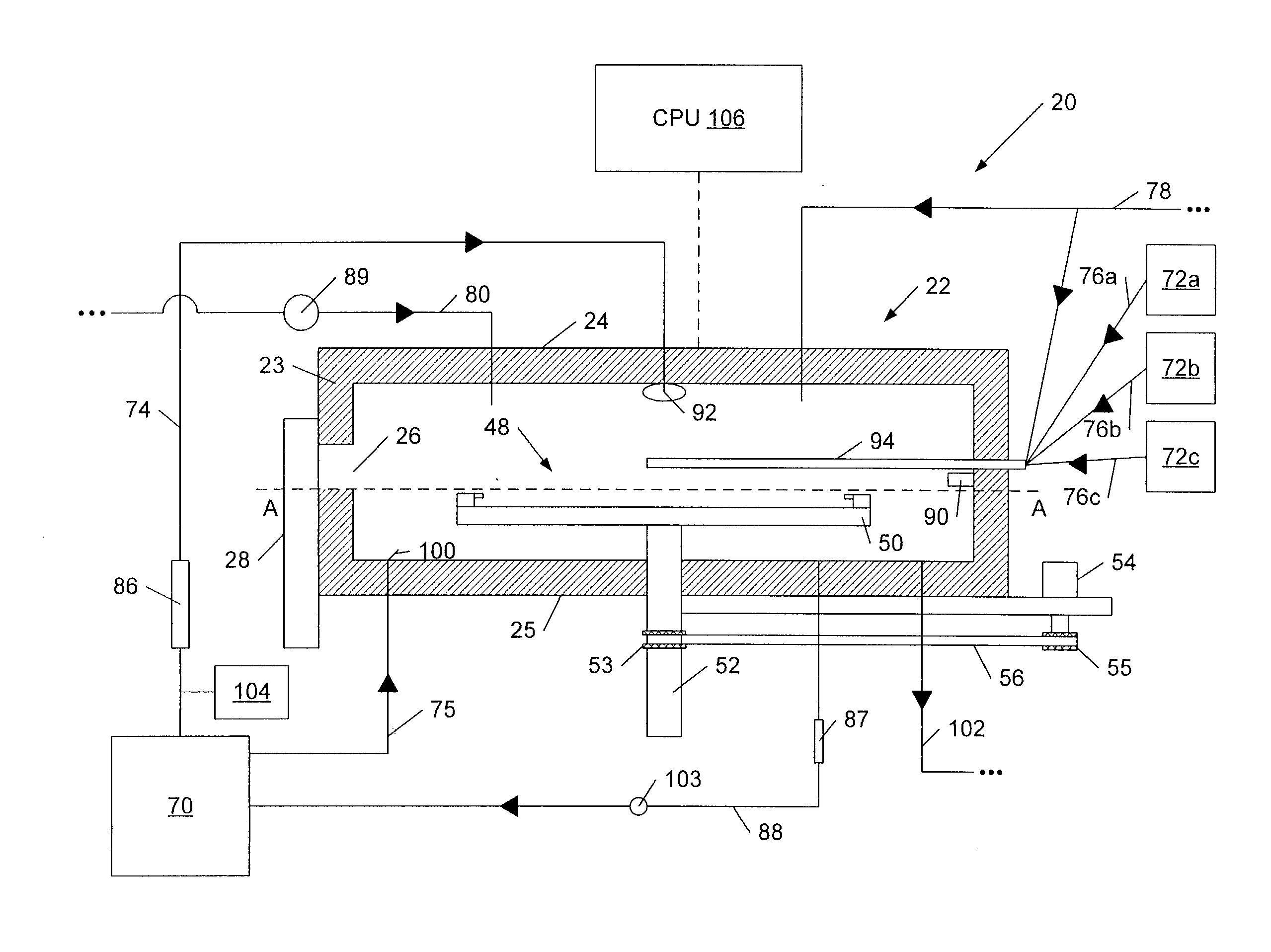
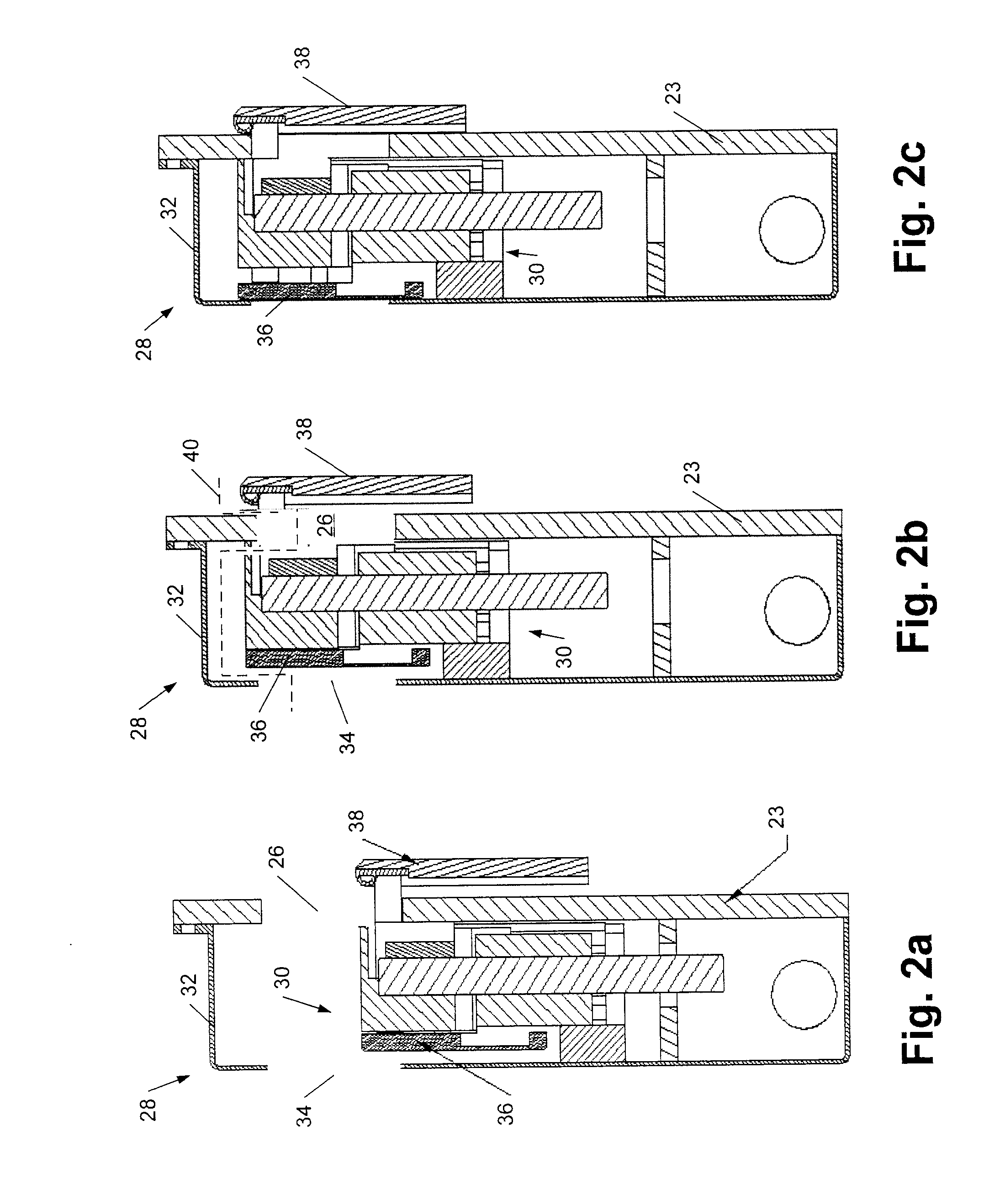
[0070]Turning now to the drawings, exemplary embodiments of systems and methods for processing a microelectronic topography are illustrated in FIGS. 1-18. More specifically, FIG. 1 illustrates an exemplary embodiment of a system that may be used for processing a microelectronic topography, while FIGS. 2a-10 show detailed illustrations of particular components of the system in FIG. 1 as well as methods of using such a system. Furthermore, FIGS. 11-18 illustrate a method for processing a microelectronic topography which may be conducted using the system shown in FIG. 1 or any other system adapted for such a method. It is noted that the plurality of component designs and methods illustrated in FIGS. 1-18 are not co-dependent and, therefore, may not necessarily be employed together. In particular, the system described herein may be constructed to include any combination of the components described in reference to FIGS. 1, 2a-2c, 4, 6a-6d, 8a, 8b, and 9a-9c. In addition, the methods for ...


PUM

PropertyMeasurementUnit
temperatureaaaaaaaaaa
thicknessaaaaaaaaaa
deposition rateaaaaaaaaaa

Abstract

A method is provided which includes forming a metal layer and converting at least a portion of the metal layer to a hydrated metal oxide layer. Another method is provided which includes selectively depositing a dielectric layer upon another dielectric layer and selectively depositing a metal layer adjacent to the dielectric layer. Consequently, a microelectronic topography is formed which includes a metal feature and an adjacent dielectric portion comprising lower and upper layers of hydrophilic and hydrophobic material, respectively. A topography including a metal feature having a single layer with at least four elements lining a lower surface and sidewalls of the metal feature is also provided herein. The fluid / s used to form such a single layer may be analyzed by test equipment configured to measure the concentration of all four elements. In some cases, the composition of the fluid / s may be adjusted based upon the analysis.

Description

CONTINUING DATA[0001]The present application is a divisional from U.S. patent application Ser. No. 10 / 462,343 filed Jun. 16, 2003.BACKGROUND OF THE INVENTION[0002]1. Field of the Invention[0003]This invention generally relates to microelectronic processing, and more particularly to the formation and processing of diffusion barrier layers.[0004]2. Description of the Related Art[0005]The following descriptions and examples are not admitted to be prior art by virtue of their inclusion within this section.[0006]Electroless plating is a process for depositing materials on a catalytic surface from an electrolyte solution without an external source of current. An advantage of an electroless deposition process is that it can be selective, i.e., the material can be deposited only onto areas that demonstrate appropriate chemical properties. In particular, local deposition can be performed onto metals that exhibit an affinity to the material being deposited or onto areas pretreated or pre-acti...

Claims


Application Information

Patent Timeline
Patent Type & Authority Applications(United States)
IPC IPC(8): B32B15/00B32B3/02B05D5/12B05D3/06B05C11/00C23C8/02C23C18/18C23C28/00H01L21/288H01L21/302H01L21/321H01L21/461H01L21/768
CPCC23C8/02Y10T428/23H01L21/288H01L21/321H01L21/76843H01L21/76849H01L21/76855H01L21/76856H01L21/76864H01L21/76874C23C18/1605C23C18/1632C23C18/1683C23C18/1803H01L21/64C23C28/321C23C28/322C23C28/34C23C28/345C23C28/3455Y10T428/24628Y10T428/12493Y10T428/12549Y10T428/1241C23C28/00
Inventor IVANOV, IGOR C.ZHANG, WEIGUOKOLICS, ARTUR
Owner LAM RES CORP
Why Eureka
Try Eureka