Semiconductor Wafer Monitoring Apparatus and Method

a technology of semiconductor wafers and monitoring apparatuses, applied in special data processing applications, instruments, electric digital data processing, etc., can solve problems such as processing problems, and achieve the effect of increasing the efficiency and throughput of metrology apparatus

Inactive Publication Date: 2011-01-20
METRYX
View PDF10 Cites 26 Cited by
  • Summary
  • Abstract
  • Description
  • Claims
  • Application Information

AI Technical Summary

Benefits of technology

[0014]The present application discloses two techniques which can increase the efficiency and throughput of metrology apparatus in a semiconductor wafer fabrication process.

Problems solved by technology

Problems in processing can be picked up using such measurements.

Method used


Image

  • Semiconductor Wafer Monitoring Apparatus and Method
  • Semiconductor Wafer Monitoring Apparatus and Method
  • Semiconductor Wafer Monitoring Apparatus and Method

Examples


Embodiment Construction

; FURTHERS OPTIONS AND PREFERENCES

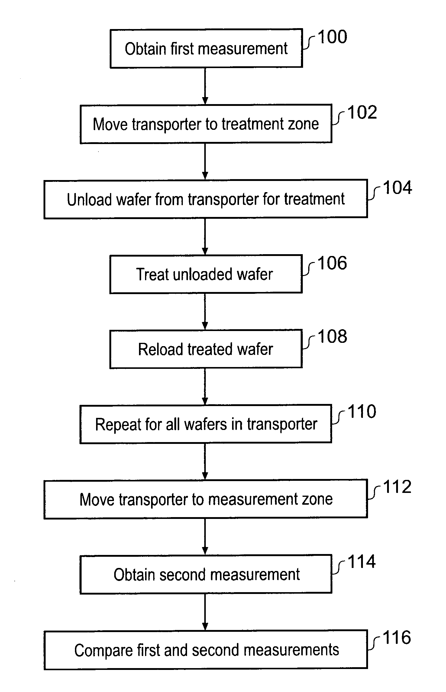
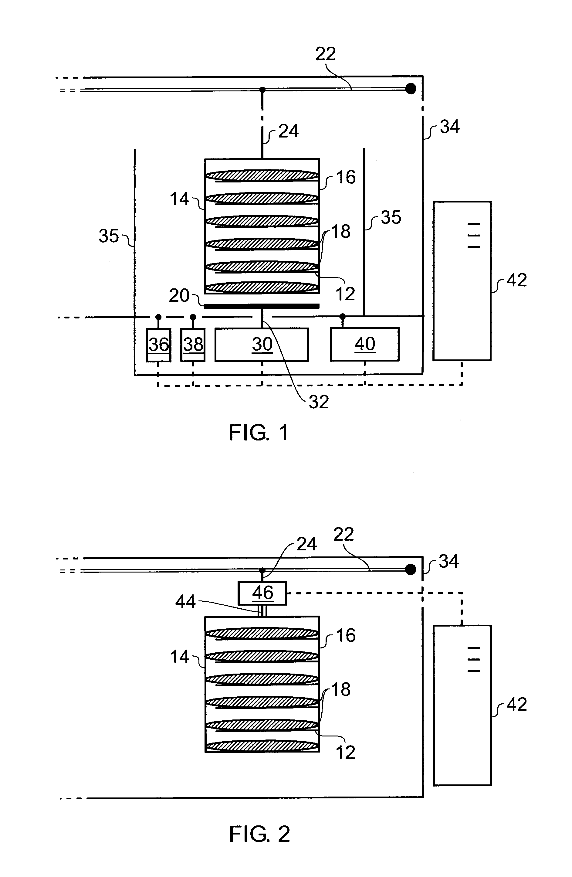
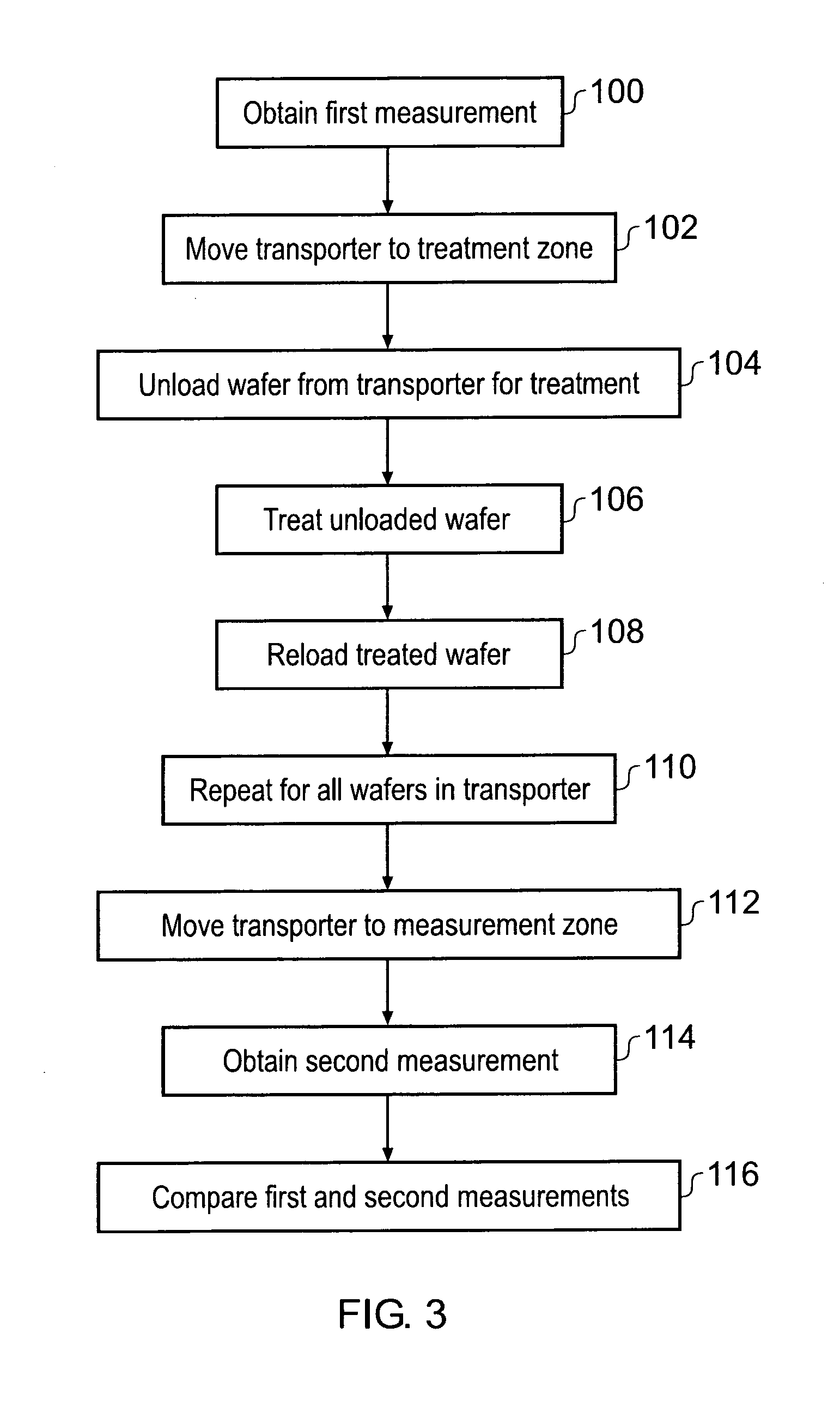
[0063]FIG. 1 shows a schematic view of part of a semiconductor wafer processing plant. The plant comprises a chamber (e.g. “clean room”) 34 in which a transporter unit (which in this embodiment is a FOUP) 16 (typically a plurality of such units) carry semiconductor wafers 18 between processing equipment (not shown) and metrology apparatus (discussed below). In this embodiment, the transporter unit 16 is a FOUP attached to an overhead rail 22 via an attachment arm 24. The FOUP 16 has a front door 14 which is openable into a cavity containing a plurality of shelves 12, each shelf 12 being arranged securely to retain a semiconductor wafer 18. When the front door 14 is closed the cavity in the FOUP 16 is protected from the environment in the chamber 34.

[0064]The overhead rail 22 may be part of a automated material handling system (AMHS) which controls automatically the movement of transporter units within the chamber 34. Such systems are already known f...


PUM


Abstract

Metrology methods and apparatus for semiconductor wafer fabrication in which data for metrology is obtained by detecting a measurable property of a monitored entity, which is either (i) a wafer transporter (e.g. a FOUP) loaded with one or more wafers to be monitored, or (ii) a plurality of wafers. Performing metrology measurements on a loaded wafer transporter enables the step of extracting wafer (s) from the transporter for metrology measurements to be omitted. Moreover, metrology measurement may be obtained while transporting the wafer (s) between treatment locations. By considering a plurality of wafers as a unit, a single measurement representing a combination of individual wafer responses is obtained. All wafers contribute to the metrology measurement without the need to perform individual wafer measurements.

Description

FIELD OF THE INVENTION[0001]This invention relates to semiconductor wafer metrology.BACKGROUND TO THE INVENTION[0002]Microelectronic devices are fabricated on semiconductor wafers using a variety of techniques, e.g. including deposition techniques (CVD, PECVD, PVD, etc) and removal techniques (e.g. chemical etching, CMP, etc). Semiconductor e.g. silicon wafers may be further treated in ways that alter their mass e.g. by cleaning, ion implantation, lithography and the like.[0003]Depending on the device being manufactured, each wafer may be passed sequentially through hundreds of different processing steps to build up and / or to remove the layers and materials necessary for its ultimate operation. In effect, each wafer is passed down a production line. The nature of semiconductor manufacturing means that certain processing steps or sequences of steps in the production flow may be repeated in a similar or identical fashion. For example, this may be to build up similar layers of metal co...

Claims


Application Information

Patent Timeline
Patent Type & Authority Applications(United States)
IPC IPC(8): G06F19/00
CPCH01L21/67253
Inventor WILBY, ROBERT JOHN
Owner METRYX
Why Eureka
Try Eureka