Semiconductor light-emitting device and method for manufacturing the same

a technology of semiconductors and light-emitting devices, which is applied in the direction of semiconductor/solid-state device manufacturing, semiconductor devices, and electrical equipment, etc., can solve the problems of pad electrodes not being able to ensure tensile stress, pad electrodes may be peeled off, etc., and achieve high and stable light-emitting output and high luminance

Inactive Publication Date: 2011-01-27
TOYODA GOSEI CO LTD
View PDF12 Cites 44 Cited by
  • Summary
  • Abstract
  • Description
  • Claims
  • Application Information

AI Technical Summary

Benefits of technology

[0015]According to the present invention, it is possible to provide a semiconductor light-emitting device in which a light emission output is high and stable. According to the present invention, it is also possible to provide high luminance semiconductor light-emitting device provided with a pad electrode that is not peeled off even by tensile stress during bonding wire junction.
[0016]In particular, since the present invention is directed to a semiconductor light-emitting device in which a bonding pad electrode has a laminate structure including a metal reflective layer and a bonding layer that are sequentially laminated from the translucent electrode side via a junction layer, and the metal reflective layer is made of at least one kind of metal selected from the group consisting of Ag, Al, Ru, Rh, Pd, Os, Ir and Pt, or an alloy containing the metal and, more preferably, the junction layer is made of at least one kind selected from the group consisting of Al, Ti, V, Cr, Mn, Co, Zn, Ge, Zr, Nb, Mo, Ru, Hf, Ta, W, Re, Rh, Ir, Ni, TiN and TaN, the effects remarkably excellent in the number of defective bondings a defect rate under a high-temperature and high-humidity test are obtained.

Problems solved by technology

However, in a light-emitting device in which metal oxide such as ITO is used as a p-type electrode and a reflective film made of Ag is used as a pad electrode, a trial of making a junction of a bonding wire to the pad electrode is made, the pad electrode can not ensure tensile stress during bonding wire junction, and thus the pad electrode may be peeled off.

Method used


Image

  • Semiconductor light-emitting device and method for manufacturing the same
  • Semiconductor light-emitting device and method for manufacturing the same
  • Semiconductor light-emitting device and method for manufacturing the same

Examples


example 1

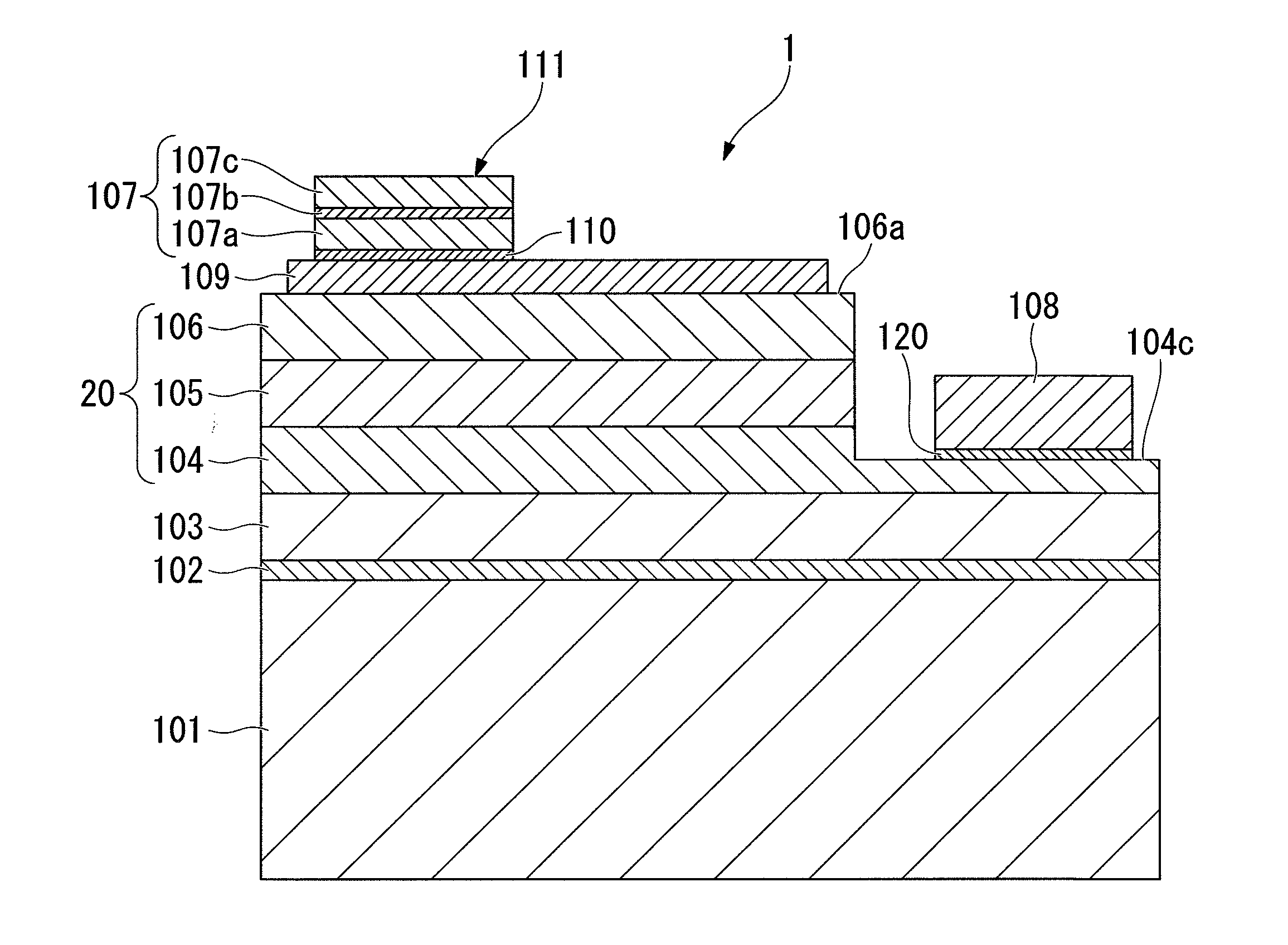
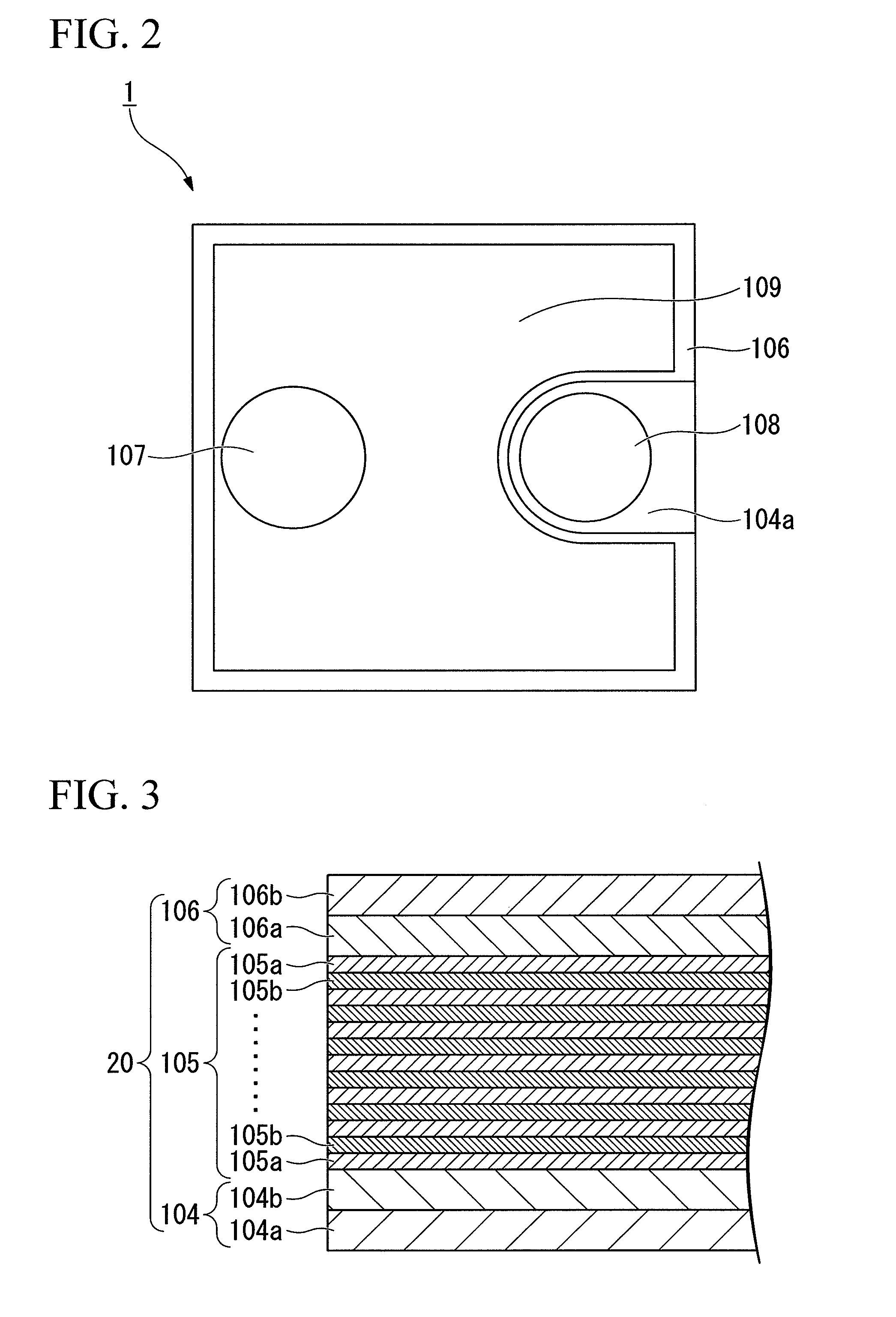
[0159]Semiconductor light-emitting devices made of nitride gallium-based compound semiconductors shown in FIG. 1 to FIG. 3 were manufactured. In the semiconductor light-emitting device of Example 1, on a substrate 101 made of sapphire, a 8 μm thick ground layer 103 made of undoped GaN, a 2 μm thick Si-doped n-type GaN contact layer 104a, a 250 nm thick n-type In0.1Ga0.9N clad layer 104b, a 16 nm thick Si-doped GaN barrier layer and a 2.5 nm thick In0.2Ga0.8N well layer were laminated five times through a buffer layer 102 made of AlN. Finally, a light-emitting layer 105 having a multiple quantum well structure provided with a barrier layer, a 10 nm thick Mg-doped p-type Al0.07Ga0.93N clad layer 106a and a 150 nm thick Mg-doped p-type GaN contact layer 106b were sequentially laminated.

[0160]Furthermore, on the p-type GaN contact layer 106b, a 200 nm thick translucent electrode 109 made of ITO and a 10 Å thick junction layer 110 made of Cr were formed by a commonly known photolithograp...


PUM


Abstract

A semiconductor light-emitting device of the present invention includes: a substrate (101); a laminate semiconductor layer (20) including a light-emitting layer (105) formed on the substrate (101); a translucent electrode (109) formed on a top surface of the laminate semiconductor layer (20); and a junction layer (110) and a bonding pad electrode (107) formed on the translucent electrode (109), wherein the bonding pad electrode (107) has a laminate structure including a metal reflective layer (107a) and a bonding layer (107c) that are sequentially laminated from the translucent electrode (109) side, and the metal reflective layer (107a) is made of at least one kind of metal selected from the group consisting of Ag, Al, Ru, Rh, Pd, Os, Ir and Pt, or an alloy containing the metal.

Description

TECHNICAL FIELD[0001]The present invention relates to a semiconductor light-emitting device and a method for manufacturing the same, and more particularly to a semiconductor light-emitting device provided with a bonding pad electrode, and a method for manufacturing the same.[0002]The present invention claims priority on Japanese Patent Application No. 2008-64716 filed on Mar. 13, 2008 in Japan and Japanese Patent Application No. 2008-117866 filed on Apr. 28, 2008 in Japan, the contents of which are incorporated herein by reference.BACKGROUND ART[0003]In recent years, GaN-based compound semiconductor materials have become of interest as a semiconductor material for a light-emitting device that emits light of short wavelength. A GaN-based compound semiconductor is formed on a substrate of a sapphire single crystal, various oxides, or a Group III-V compound, through thin-film forming means such as a metal-organic chemical vapor deposition method (MOCVD method), a molecular-beam epitaxy...

Claims


Application Information

Patent Timeline
Patent Type & Authority Applications(United States)
IPC IPC(8): H01L33/42H01L33/32H01L33/40
CPCH01L33/32H01L33/42H01L33/405H01L2924/181H01L2224/48091H01L2224/48247H01L2224/48257H01L2224/49107H01L2224/45144H01L2924/00012H01L2924/00014H01L2924/00
Inventor OKABE, TAKEHIKOHIRAIWA, DAISUKENAKATA, MASATOMIKI, HISAYUKIFUKUNAGA, NAOKISHINOHARA, HIRONAO
Owner TOYODA GOSEI CO LTD
Why Eureka
Try Eureka