Amplifier, Optical Receiver Circuit, Optical Module and Data Exchange System

a technology of optical receiver circuit and amplifier, which is applied in the direction of amplifiers with field-effect devices, electromagnetic transmission, electromagnetic transceivers, etc., can solve the problems of difficult circuit system to inhibit power supply noise, and achieve the effect of reducing power supply noise and low area requirements

Inactive Publication Date: 2011-01-27
HITACHI LTD
View PDF7 Cites 9 Cited by
  • Summary
  • Abstract
  • Description
  • Claims
  • Application Information

AI Technical Summary

Benefits of technology

[0013]Referring to Equation 1, the amount of superimposed power supply noise can be reduced by decreasing the values gm2 and ro. However, the values gm2 and ro are constants determined by a process and cannot be decreased with ease. Therefore, it is difficult to reduce the noise.
[0014]The noise rejection method for use with a receiver that is disclosed in Japanese Patent Application Laid-Open Publication No. S59-115628 aims to eliminate noise from a signal. However, this method entails the use of two receiver circuits in order to achieve noise signal detection and noise rejection. In addition, this method also entails the use of a phase inverter and an adder circuit. Consequently, the use of this method considerably increases the circuit area and makes it difficult to provide a multichannel capability.
[0015]The present invention has been made in view of the above circumstances, and provides an optical receiver circuit that addresses the problems with the related art described above and reduces the amount of power supply noise superimposed on a signal with low area requirements.
[0017]The present invention provides an amplifier, an optical receiver circuit, an optical module, and a data exchange system that make it possible to reduce the amount of power supply noise superimposed on a signal with low area requirements.

Problems solved by technology

However, it is difficult for this circuit system to inhibit power supply noise from being superimposed on a signal.

Method used


Image

  • Amplifier, Optical Receiver Circuit, Optical Module and Data Exchange System
  • Amplifier, Optical Receiver Circuit, Optical Module and Data Exchange System
  • Amplifier, Optical Receiver Circuit, Optical Module and Data Exchange System

Examples


first embodiment

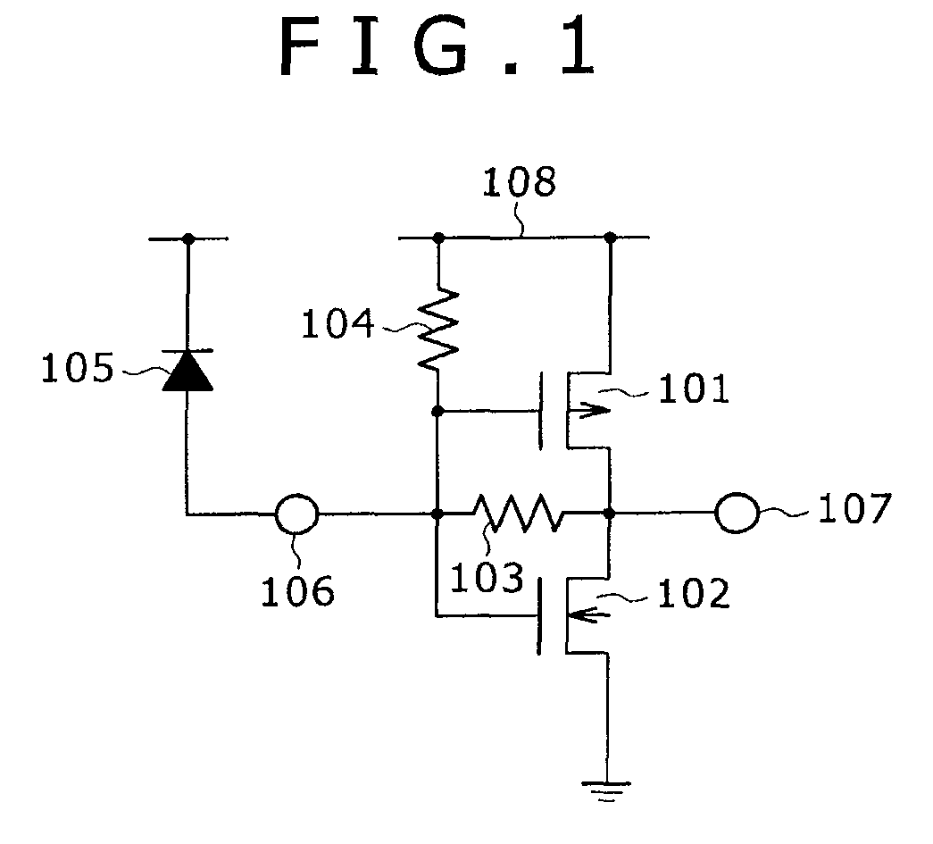
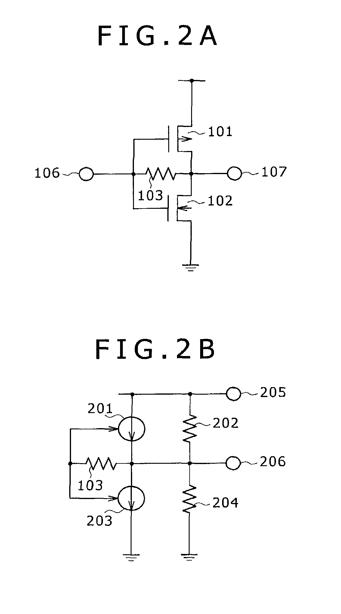
[0037]FIGS. 3A and 3B show an example of an amplifier according to a first embodiment of the present invention. FIG. 3A is a schematic circuit diagram illustrating the amplifier according to the first embodiment of the present invention. FIG. 3B is a diagram illustrating a small signal equivalent circuit that represents a signal path between an output terminal and a power supply for the amplifier shown in FIG. 3A.

[0038]The amplifier shown in FIG. 3A includes a CMOS inverter, resistors 103, 104, an input terminal 106, an output terminal 107, and a power supply 108. The CMOS inverter includes a PMOS transistor 101 and an NMOS transistor 102. The resistor 103 is placed in a feedback path that is extended from the output terminal 107 of the CMOS inverter to the input terminal 106, and forms a shunt feedback signal amplifier. The resistor 104 is positioned between the input terminal 106 and the power supply 108. As the resistor 104 is positioned in such a manner, two paths are formed for...

second embodiment

[0047]FIG. 6 is a schematic circuit diagram illustrating an example of the amplifier according to a second embodiment of the present invention. The amplifier according to the second embodiment differs from the amplifier according to the first embodiment in that a resistor 124 for noise rejection is connected to a ground. The noise rejection resistor 124 is provided to form two noise paths that transmit ground noise to the output terminal 107. One noise path 804 transmits the ground noise to the output terminal 107 through the NMOS transistor 102. The other noise path 803 transmits the ground noise to the output terminal 107 through the resistor 124 and then the PMOS transistor 101. The noise path 804 is of a common gate type that inputs noise into the source of the NMOS transistor 102 and outputs the noise to the drain. Therefore, the phase of the ground noise is the same as the phase transmitted to the output terminal 107. On the other hand, the noise path 803 is of a common source...

third embodiment

[0048]FIGS. 7A and 7B are diagrams illustrating examples of the amplifier according to a third embodiment of the present invention. More specifically, FIGS. 7A and 7B show modifications of the amplifier according to the third embodiment of the present invention.

[0049]The configuration of the amplifier shown in FIG. 7A is characterized in that the resistor 104 shown in FIG. 3A is replaced by a variable resistor 134. The configuration of the amplifier shown in FIG. 7B is characterized in that the resistor 124 shown in FIG. 6 is replaced by a variable resistor 144. In the third embodiment, a variable resistor is used instead of a resistor. The employed variable resistor 134 or variable resistor 144 is used for noise rejection. These variable resistors 134, 144 can change the amount of superimposed noise and provide adjustability even when variation occurs in the elements in the amplifier. Further, the above-described effect can be achieved with a low-area amplifier.


PUM


Abstract

When a conventional optical receiver circuit is used, it is difficult to achieve noise reduction or provide a multichannel capability due to a considerable circuit area increase. Disclosed is an amplifier for optical communications that includes a CMOS inverter, which has a PMOS transistor and an NMOS transistor; an input terminal, which inputs a signal into the CMOS inverter; an output terminal, which outputs a signal from the CMOS inverter; a power supply, which is connected to the CMOS inverter; a first element and a second element, which are respectively connected to the CMOS inverter; and two types of power supply paths, which are in opposite phase to each other.

Description

INCORPORATION BY REFERENCE[0001]This application claims the benefit of priority from Japanese Patent Application No. JP2009-170711 filed on Jul. 22, 2009, entitled “AMPLIFIER, OPTICAL RECEIVER CIRCUIT, OPTICAL MODULE, AND DATA EXCHANGE SYSTEM,” the entire contents of which are incorporated herein by reference.BACKGROUND OF THE INVENTION[0002](1) Field of the Invention[0003]The present invention relates to an amplifier capable of reducing the influence of power supply noise, an optical receiver circuit that uses the amplifier, an optical module that uses the amplifier, and a data exchange system that uses the amplifier.[0004](2) Description of the Related Art[0005]In recent years, the traffic capacity required for a network has increased at an accelerated pace due to recent widespread use of the Internet. In the field of backplane transmission within the housing of a server, router, or other large-capacity data transmission device for a computer, telecommunication apparatus, or the l...

Claims


Application Information

Patent Timeline
Patent Type & Authority Applications(United States)
IPC IPC(8): H04B10/00H03F3/16H04B10/06H03F3/08H04B10/2507H04B10/40H04B10/50H04B10/60H04B10/69
CPCH04B10/693H03F3/08
Inventor YAZAKI, TORU
Owner HITACHI LTD
Why Eureka
Try Eureka