Liquid crystal display device, semiconductor device, and electronic appliance

a liquid crystal display and semiconductor technology, applied in semiconductor devices, semiconductor/solid-state device details, instruments, etc., can solve the problems of increased manufacturing cost and number of manufacturing steps, and achieve the effect of low manufacturing cost and wide viewing angl

Active Publication Date: 2011-02-10
SEMICON ENERGY LAB CO LTD
View PDF99 Cites 110 Cited by
  • Summary
  • Abstract
  • Description
  • Claims
  • Application Information

AI Technical Summary

Benefits of technology

[0007]As described above, in the case of employing a structure in which the second electrode (such as the common electrode) is located under the first electrode (such as the pixel electrode), both the common electrode and the pixel electrode are formed of ITO conventionally. Accordingly, the numbers of manufacturing steps and masks, and manufacturing cost have been increased. The present invention is made in view of the foregoing, and an object of the present invention is to provide a liquid crystal display device and an electronic appliance with wide viewing angle, having less numbers of manufacturing steps and masks and low manufacturing cost compared with a conventional device; and to provide a manufacturing method of the liquid crystal display device.

Problems solved by technology

Accordingly, the numbers of manufacturing steps and masks, and manufacturing cost have been increased.

Method used


Image

  • Liquid crystal display device, semiconductor device, and electronic appliance
  • Liquid crystal display device, semiconductor device, and electronic appliance
  • Liquid crystal display device, semiconductor device, and electronic appliance

Examples


embodiment mode 1

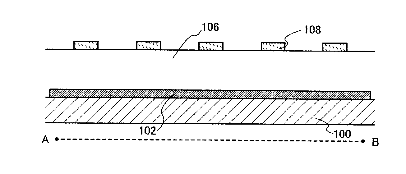
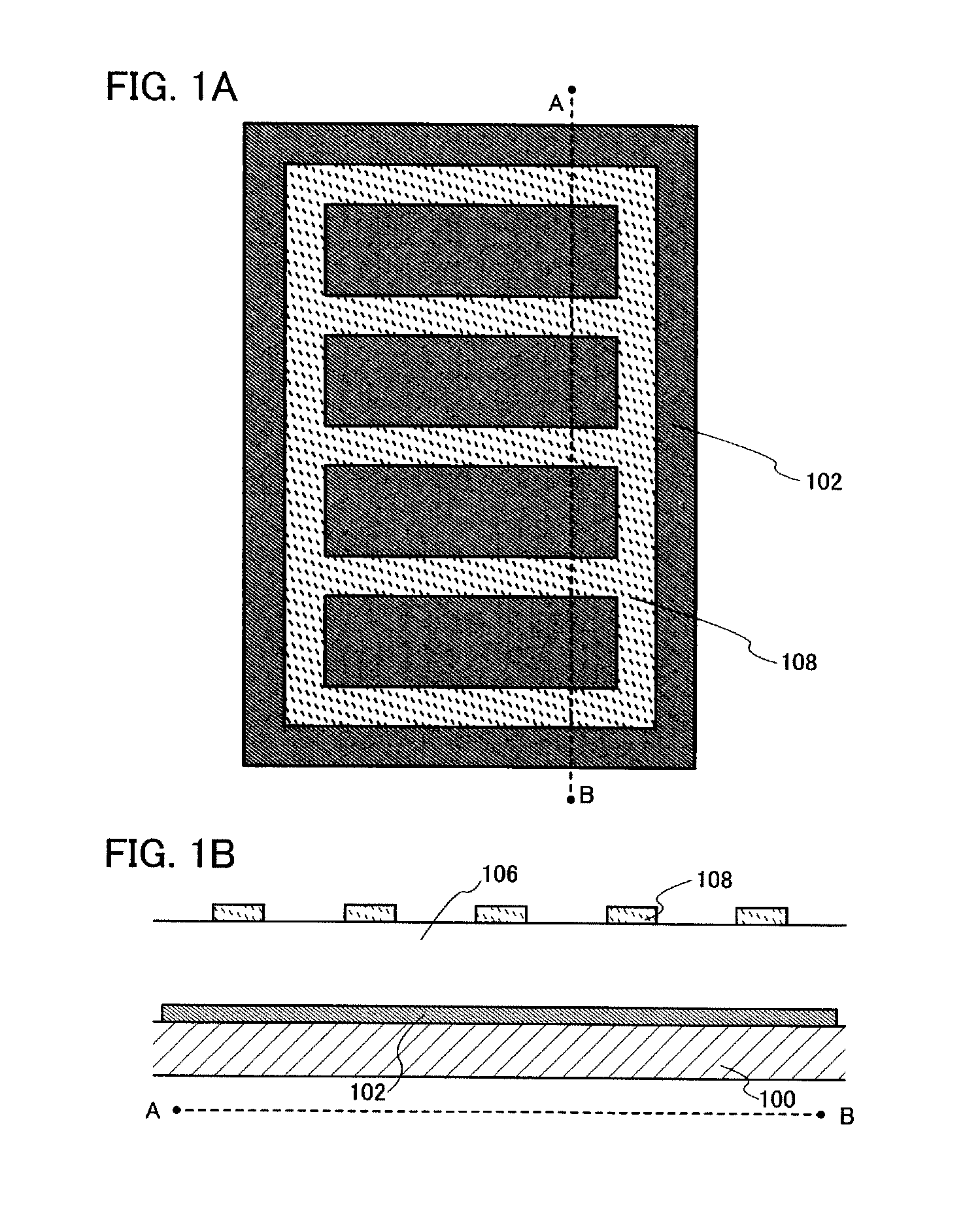
[0085]FIGS. 1A and 1B illustrate a basic example of the present invention. FIG. 1A is a plan view and FIG. 1B is a cross-sectional view.

[0086]A first electrode 102 is formed over a substrate 100. The first electrode 102 is formed with use of ITO (indium tin oxide) conventionally.

[0087]In the present invention, the first electrode 102 is formed of, for example, a semiconductor material containing silicon, although not limited thereto. Alternatively, amorphous silicon may be used but in order to enhance conductivity, polysilicon (polycrystalline silicon), single crystalline silicon, and the like may be used. Further, in many cases, the first electrode contains an impurity (a p-type impurity or an n-type impurity) such as phosphorus, boron, gallium, or arsenic to further enhance the conductivity.

[0088]The reason of using a semiconductor material containing silicon for the first electrode 102 is that silicon has high transmittance. In addition, since the first electrode 102 is thin, it ...

embodiment mode 2

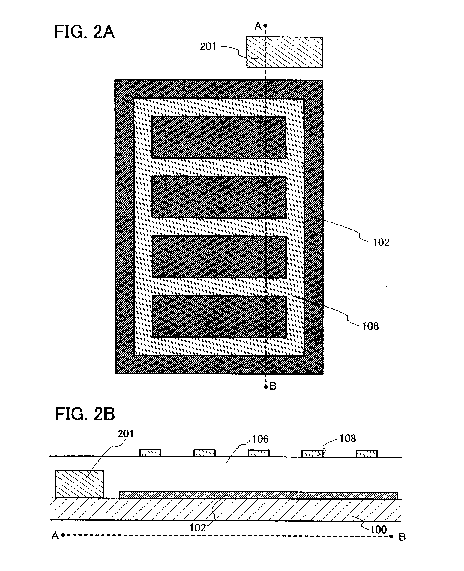
[0182]FIG. 9A is a plan view illustrating a structure of an FFS mode liquid crystal display device according to Embodiment Mode 2 in the present invention. FIG. 9B is a cross-sectional view along a line A-B and a line C-D of FIG. 9A. A structure of this embodiment mode is similar to that of Embodiment Mode 1, except that the first electrode 102c is electrically connected to the source wiring 107a through the transistor and functions as the pixel electrode, the second electrode 108 is electrically connected to the auxiliary wiring 104b and functions as the common electrode, a shape of the opening pattern 112 formed in the second electrode 108 is different, and connection structures of the first electrode 102c, the second electrode 108, and the wirings are different. Also, a manufacturing method of the liquid crystal display device according to this embodiment mode is almost similar to that in Embodiment Mode 1. Therefore, the description in Embodiment Mode 1 can be applied to this em...

embodiment mode 3

[0194]FIG. 10A is a plan view illustrating a structure of a liquid crystal display device according to Embodiment Mode 3 in the present invention. FIG. 10B is a cross-sectional view along a line A-B, a line C-D, and a line E-F of FIG. 10A. A structure of this embodiment mode is similar to that of Embodiment Mode 1, except that an opening pattern 115 is formed in the first electrode 102c and except for the shape of the opening pattern 112. In other words, the liquid crystal display device according to this embodiment mode is a device in which the alignment direction of the liquid crystal is controlled by an IPS mode. The pixel portion and the common electrode are alternately arranged and are generally in parallel in a main portion, when seen from a direction perpendicular to the substrate 100 of the liquid crystal display device. In the aforementioned FFS mode, a lower electrode of the pixel electrode and the common electrode does not have an opening pattern. Note that a manufacturin...


PUM

PropertyMeasurementUnit
transmittanceaaaaaaaaaa
light transmittanceaaaaaaaaaa

Abstract

The liquid crystal display device includes an island-shaped first semiconductor film 102 which is formed over a base insulating film 101 and in which a source 102d, a channel forming region 102a, and a drain 102b are formed; a first electrode 102c which is formed of a material same as the first semiconductor film 102 to be the source 102d or the drain 102b and formed over the base insulating film 101; a second electrode 108 which is formed over the first electrode 102c and includes a first opening pattern 112; and a liquid crystal 110 which is provided over the second electrode108.

Description

CROSS-REFERENCE TO RELATED APPLICATIONS[0001]This application is a continuation of U.S. application Ser. No. 11 / 695,898, filed Apr. 3, 2007, now pending, which claims the benefit of a foreign priority application filed in Japan as Serial No. 2006-105618 on Apr. 6, 2006, both of which are incorporated by reference.BACKGROUND OF THE INVENTION[0002]1. Field of the Invention[0003]The present invention relates to a semiconductor device, a liquid crystal display device, and an electronic appliance including them. In particular, the present invention relates to a semiconductor device and a liquid crystal display device in which an electric field generally parallel to a substrate is generated to control liquid crystal molecules, and an electronic appliance including the semiconductor device or the liquid crystal display device.[0004]2. Description of the Related Art[0005]As one of plans for technical development of a liquid crystal display device, to widen a viewing angle can be given. As a...

Claims


Application Information

Patent Timeline
Patent Type & Authority Applications(United States)
IPC IPC(8): G02F1/1343
CPCG02F1/134363G02F1/13439G02F1/1362H01L27/124H01L2924/0002H01L2924/00G02F1/1303G02F1/1343H01L23/48H01L27/1214H01L29/40G02F1/136231G02F1/134372G02F1/133345G02F1/133514G02F1/1337G02F1/134309G02F1/136213G02F1/136286G02F1/1368H01L27/1225H01L27/1255H01L29/7869H01L29/78696
Inventor KIMURA, HAJIME
Owner SEMICON ENERGY LAB CO LTD
Why Eureka
Try Eureka