Annealing apparatus

a technology of annealing apparatus and annealing chamber, which is applied in the direction of lighting and heating apparatus, stoves or ranges, furniture, etc., can solve the problems of significant reduction of thermal resistance and sufficient thermal conductivity of adhesion parts, and achieve the effect of reducing maintenance and efficient cooling

Active Publication Date: 2011-02-10
TOKYO ELECTRON LTD
View PDF23 Cites 33 Cited by
  • Summary
  • Abstract
  • Description
  • Claims
  • Application Information

AI Technical Summary

Benefits of technology

[0006]In view of the above, the present invention provides an annealing apparatus employing a light emitting elements such as a light emittin...

Problems solved by technology

With such configuration, the adhesion parts have significantly...

Method used


Image

  • Annealing apparatus
  • Annealing apparatus
  • Annealing apparatus

Examples


Embodiment Construction

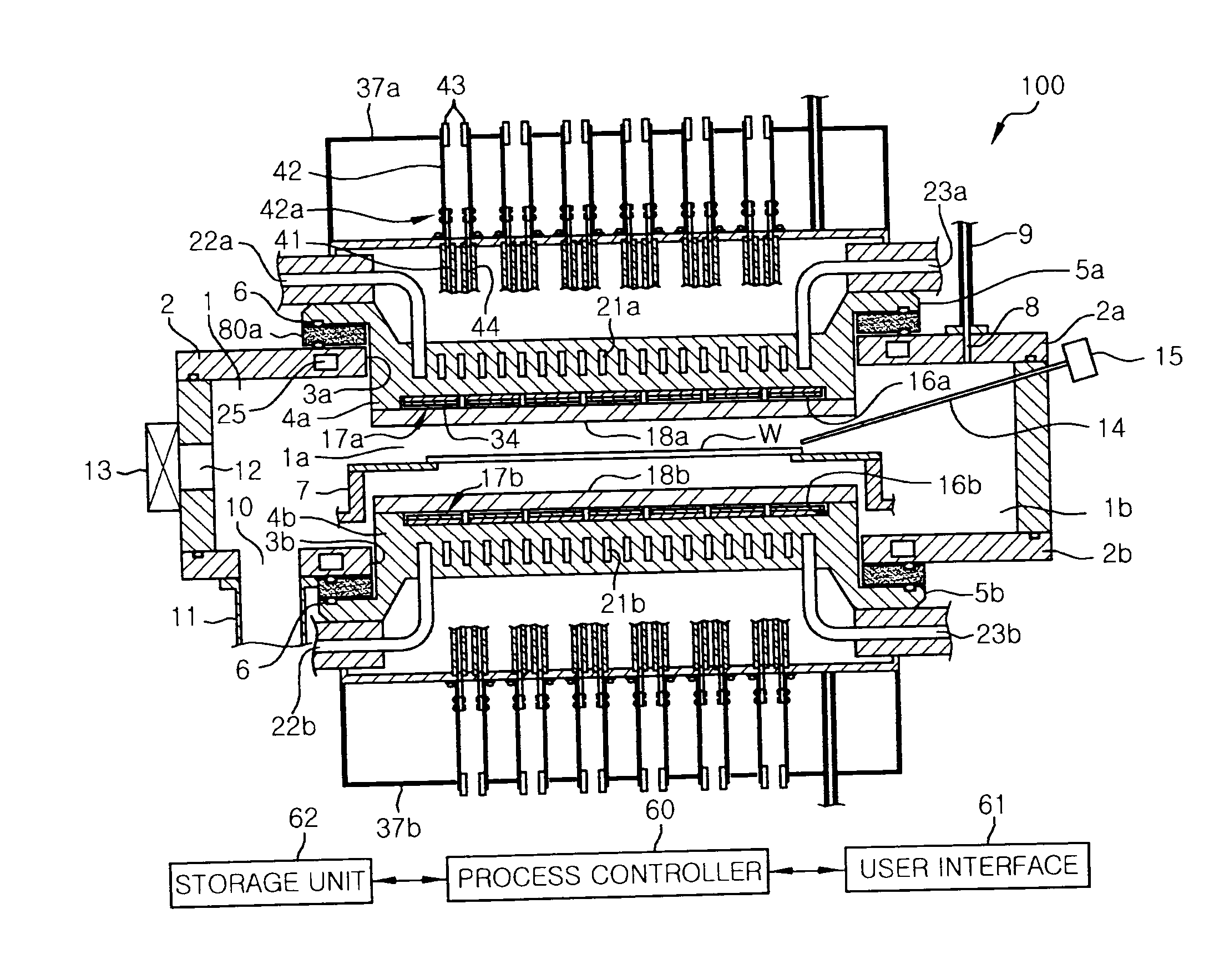
[0043]Embodiments of the present invention will now be described with reference to the accompanying drawings which form a part hereof. Here, an annealing apparatus for annealing a wafer having a surface in which impurities are implanted is taken as an example.

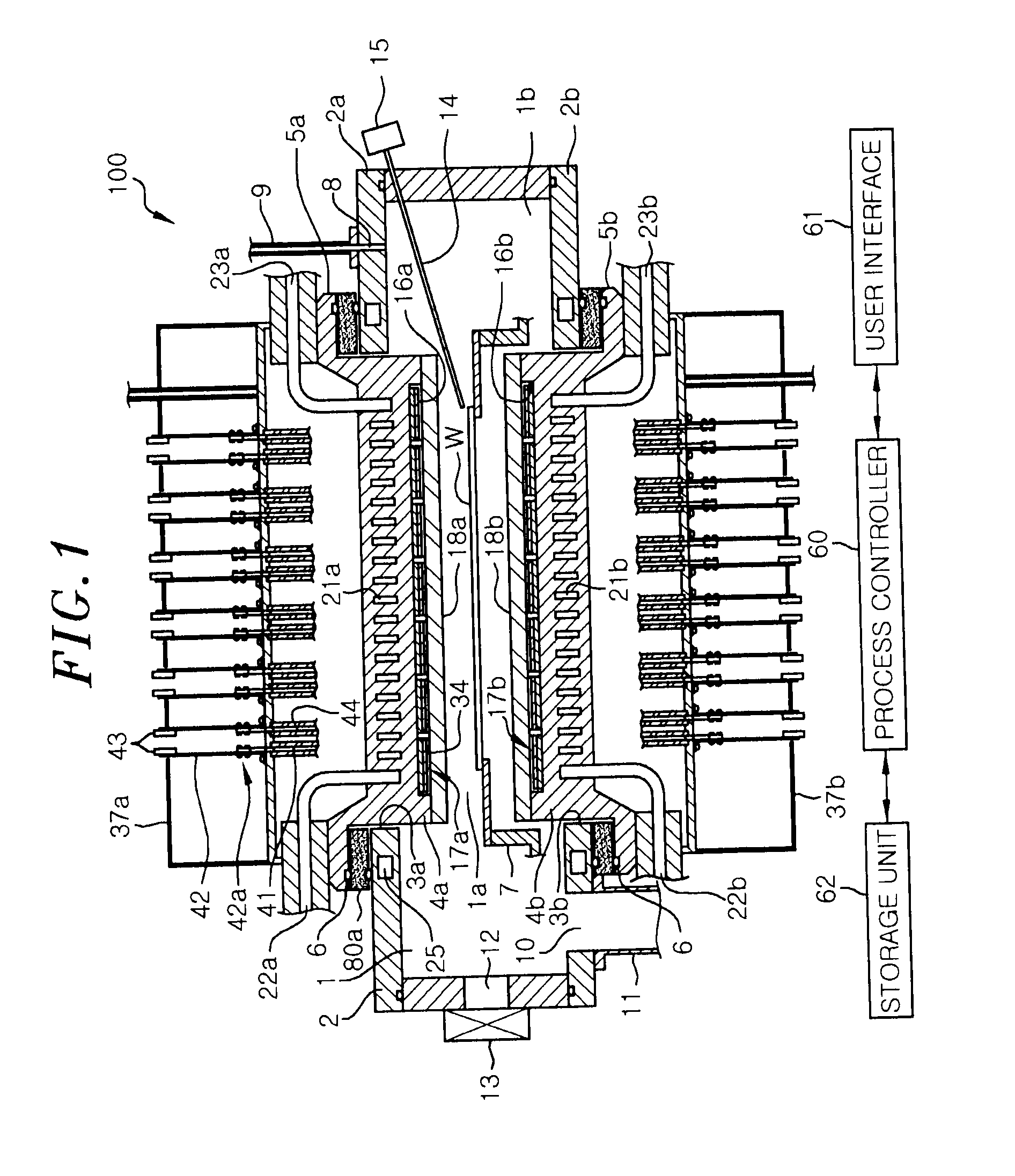
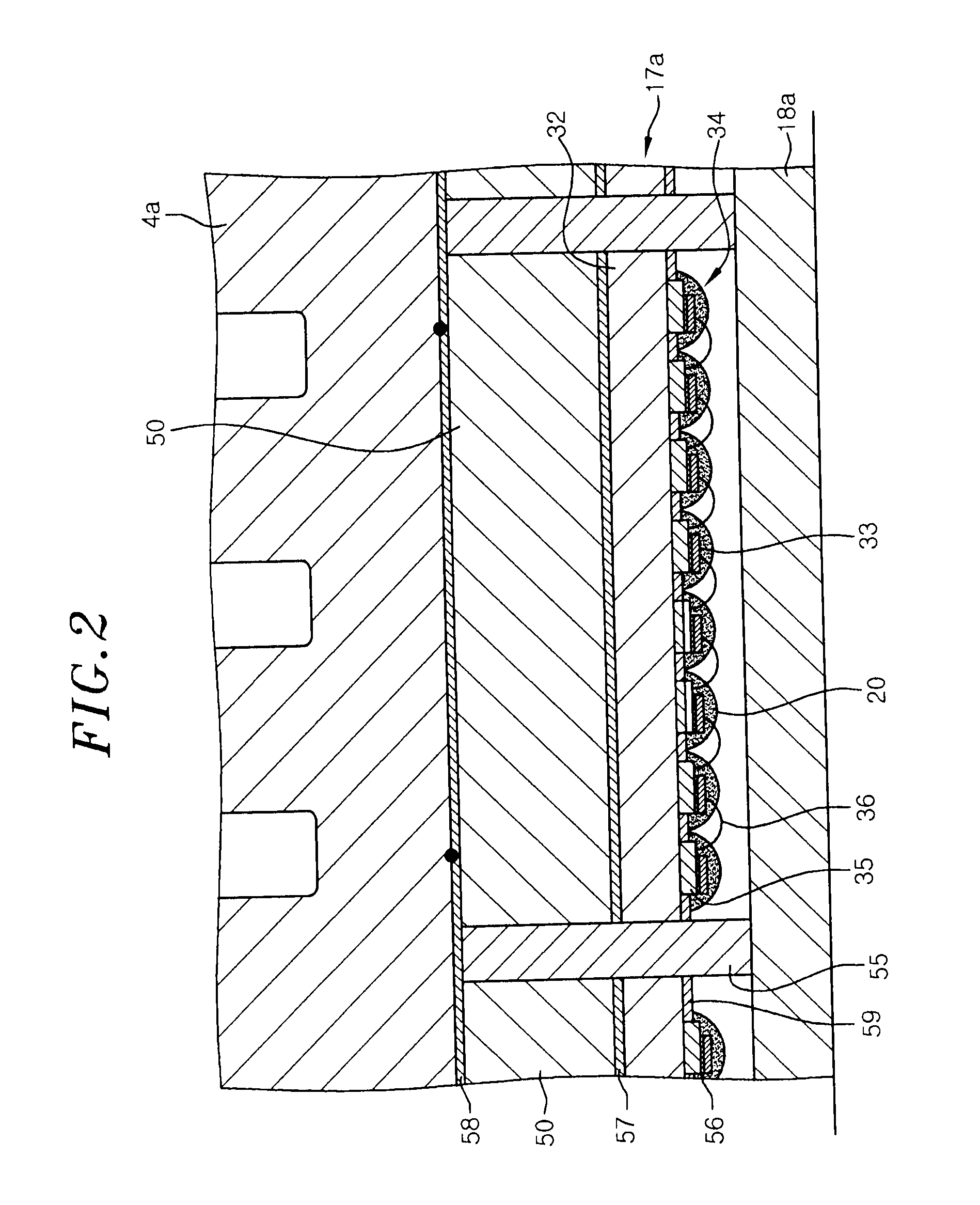
[0044]FIG. 1 is a cross sectional view showing a schematic structure of an annealing apparatus in accordance with a first embodiment of the present invention. FIG. 2 is an enlarged cross sectional view showing a heating source of the annealing apparatus shown in FIG. 1. FIGS. 3 and 4 show other examples of adhesive parts of an LED. FIG. 9 is an enlarged cross sectional view showing a part for supplying a power to an LED of the annealing apparatus shown in FIG. 1.

[0045]The annealing apparatus 100 includes an airtight processing space 1 into which a wafer W is loaded. The processing space 1 includes a cylindrical annealing portion 1a in which the wafer W is arranged and a doughnut-shaped gas diffusion portion 1b provided outside ...


PUM


Abstract

An annealing apparatus includes heating sources 17a and 17b provided to face a wafer W, the heating sources 17a and 17b having LEDs 33 emitting lights to the wafer; light-transmitting members 18a and 18b for transmitting the lights emitted from the LEDs 33; and cooling members 4a and 4b made of aluminum and provided to directly contact with the heating sources 17a and 17b, respectively. The heating sources 17a and 17b include a plurality of LED arrays having supporters 32 made of AlN, each having one surface on which the LEDs 33 are adhered by using a silver paste 56; and other surface on which thermal diffusion members 50 made of copper are adhered by using a solder 57. The LED arrays 34 are fixed to the cooling member 4a(4b) by using screws via a silicon grease.

Description

FIELD OF THE INVENTION[0001]The present invention relates to an annealing apparatus which performs an annealing process by emitting a light from a light emitting element such as a light emitting diode to a semiconductor wafer or the like.BACKGROUND OF THE INVENTION[0002]In a semiconductor device manufacturing process, a target substrate to be processed, i.e., a semiconductor wafer (hereinafter, simply referred to as a wafer), is subjected to various heat treatments such as a film forming process, an oxidation / diffusion process, a quality modification process, and an annealing process. Especially, in the annealing process after ion implantation, it is required to increase and decrease the temperature rapidly so as to minimize the diffusion, in response to the demand for the high speed and high integration of semiconductor device. There has been disclosed an annealing apparatus capable of increasing and decreasing the temperature rapidly, the annealing apparatus employing light emitti...

Claims


Application Information

Patent Timeline
IPC IPC(8): F27D11/12
CPCH01L21/268H01L21/67115H01L21/67109H01L21/324
Inventor KASAI, SHIGERUMIYASHITA, HIROYUKISUZUKI, TOMOHIROYONEDA, MASATAKEOOYA, KAZUHIRO
Owner TOKYO ELECTRON LTD
Why Eureka
Try Eureka