Optical component using composite substrate and process for producing same

a technology of composite substrates and optical components, applied in the field of process for producing optical components, can solve the problems of high cost burden, high cost, and high cost burden of substrate polishing, and achieve the effect of reducing the cost burden

Inactive Publication Date: 2011-02-17
NAT INST OF ADVANCED IND SCI & TECH
View PDF4 Cites 5 Cited by
  • Summary
  • Abstract
  • Description
  • Claims
  • Application Information

AI Technical Summary

Benefits of technology

[0032]In order to produce an optical component with a stacked thin film, in the prior art, many processes had had to be run in order to polish an optical substrate. Thus, the cost burden was high, and a huge amount of polishing techniques had had to be maintained. However, the present invention realizes the simplification of the polishing process of the optical substrate. Further, it is possible to terminate production within a relatively short time from the production of an optical substrate to the production of an optical component while maintaining high accuracy.
[0033]Further, there has been generally known that as the size of the optical substrate is increased, the polishing of the optical substrate becomes very difficult. In the prior art, polishing had had to be applied to each optical substrate, however, in the present invention, one extra-flat pressing plate may be produced relative to the required size of a substrate, whereby the required number of times of polishing can be reduced.

Problems solved by technology

The substrate polishing requires a time based on repeated polishing treatments, expensive devices and the management thereof, and a huge amount of polishing techniques.
Until now, although an extremely flat substrate has been obtained by a highly accurate polishing technique, recesses as polishing marks are locally provided on the surface of the substrate due to abrasive particles in the process of the polishing, and the recess portion causes increase in roughness.
In the local position, the poor surface state causes reduction in performances of an optical thin film and an optical component using the optical thin film.

Method used


Image

  • Optical component using composite substrate and process for producing same
  • Optical component using composite substrate and process for producing same
  • Optical component using composite substrate and process for producing same

Examples


embodiment 1

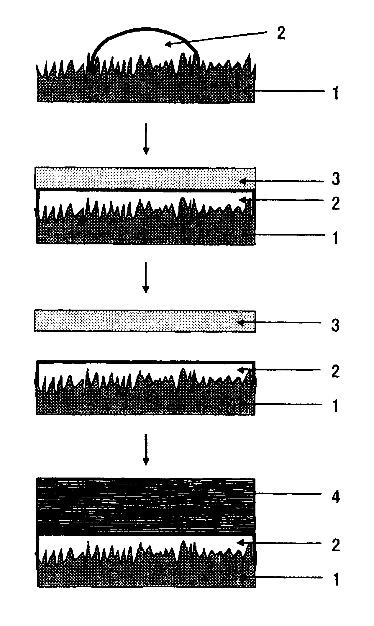
[0038]As shown in FIG. 1, an appropriate amount of an acrylic liquid photo-curable resin composition 2 (from Toyo Gosei Co., Ltd., PAK-01) was placed on an optical substrate 1 formed of borosilicate glass (trade name: BK7, surface roughness RMS=1.22 nm), and a printing pressure was applied to the resin composition 2 by using an extra-flat pressing plate 3 formed of silicon (surface roughness RMS=0.12 nm). Thereafter, light of 365 nm was applied from the optical substrate 1 side to cause a curing reaction, and the extra-flat pressing plate 3 was demolded to form a resin flat surface of the resin composition 2. The surface roughness RMS on the resin flat surface at that time is 0.21 nm, and an extra-flat composite substrate is obtained.

embodiment 2

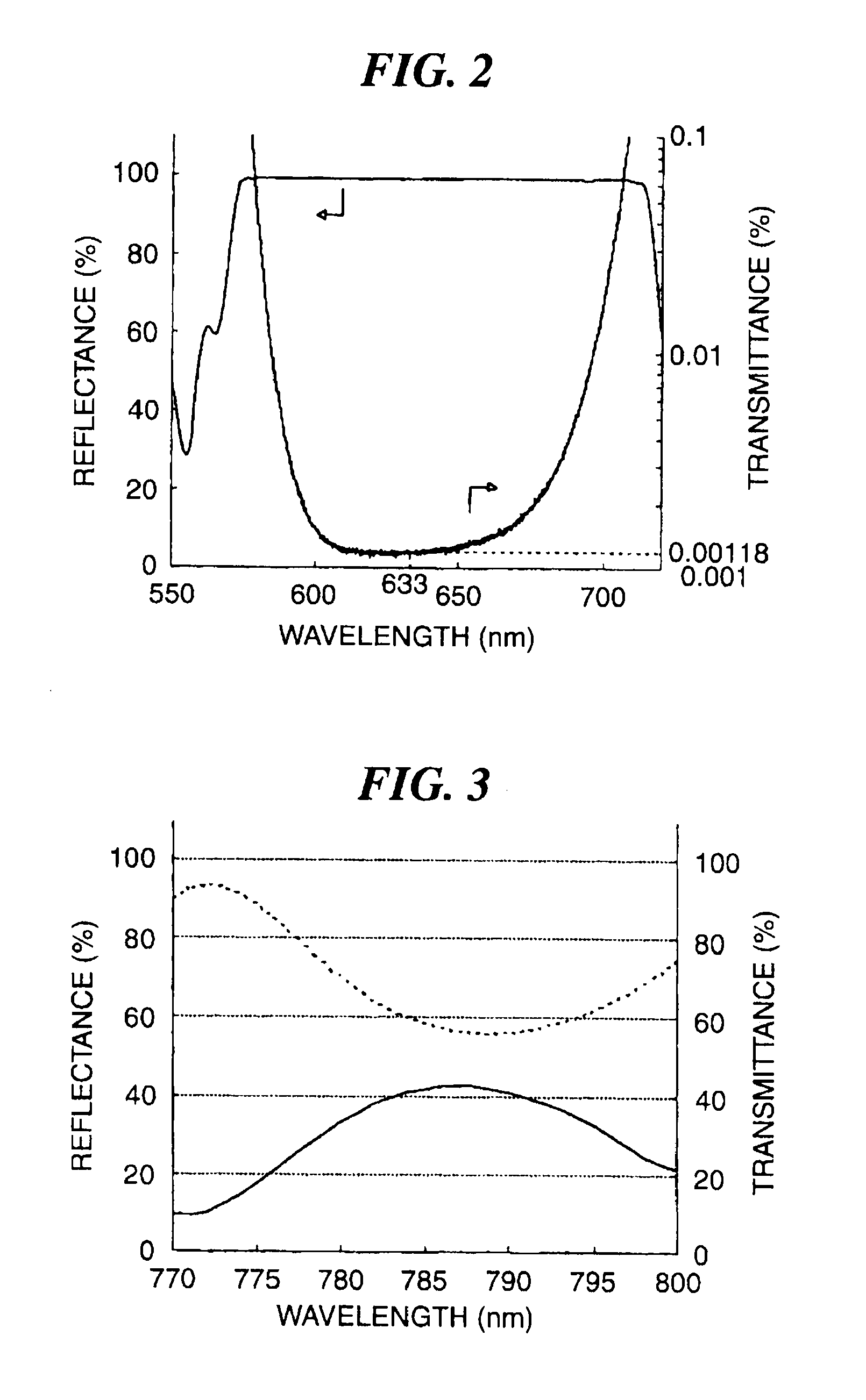
[0039]The extra-flat composite substrate obtained in Embodiment 1 is used, and oxide silicon and tantalum oxide each having a ¼ wavelength thickness were alternately stacked by an ion beam sputtering apparatus (from Veeco Instruments Inc.) to stack a dielectric multilayered optical thin film 4 having 41 layers, and, thus, to produce a highly reflection mirror for 633 nm. Consequently, the surface roughness RMS is 0.16 nm, and the results of the reflective spectrum characteristics of FIG. 2 show that the reflectance at the wavelength of 633 nm is a level extremely close to 100%. The transmittance at this time is 0.001% level, and thus it is confirmed that the transmittance is low.

embodiment 3

[0042]The composite substrate obtained in Embodiment 1 was used, and a beam splitter was produced by a similar method to Embodiment 2. Consequently, as shown in FIG. 3, when the wavelength is 787 nm, the transmittance is 57%, and the reflectance is 43%. Thus it is confirmed that the beam splitter has characteristics of a small loss.


PUM

PropertyMeasurementUnit
roughnessaaaaaaaaaa
reflectanceaaaaaaaaaa
surface roughness RMSaaaaaaaaaa

Abstract

A resin composition (2) such as a photo-curable resin composition or a heat curable or thermosetting resin composition is placed on an optical substrate (1). A printing pressure is applied to the side of the resin composition (2) of the optical substrate (1) with the resin composition (2) by means of an extra-flat pressing plate having a flatter plane than the optical substrate (1). The resin composition is cured by utilizing light or a temperature change to form a composite substrate. A thin film (4) such as a functional inorganic optical film, a dielectric multilayered optical thin film, or an optical functional metallic film is stacked on the composite substrate, for example, by low-temperature sputtering or ion beam sputtering to form an optical component such as a reflection mirror, a beam splitter, a band-pass filter, a band-stop filter, and an edge filter.

Description

TECHNICAL FIELD[0001]The present invention relates to a process for producing an optical component, which can obtain an optical component having good characteristics even if using a not highly polished optical substrate, and an optical component produced by the production process.BACKGROUND ART [0002]Currently, in the production of an optical thin film, glass of various compositions is usually used as a substrate for an optical thin film substrate, which is a raw material of the optical thin film, and the substrate has a highly polished surface. The substrate polishing requires a time based on repeated polishing treatments, expensive devices and the management thereof, and a huge amount of polishing techniques.[0003]When a functional inorganic optical film stacked on a substrate surface based on the polishing of the substrate is produced, the functional inorganic optical film has a shape reflecting the substrate surface, and there has been known that the substrate surface significan...

Claims


Application Information

Patent Timeline
Patent Type & Authority Applications(United States)
IPC IPC(8): B32B9/04C23C14/34B32B17/06B32B15/04B32B38/00B29C59/02B29L9/00B29L11/00B32B37/10G02B5/04G02B5/26G02B5/28
CPCB32B37/12B32B2037/1253B32B2037/243B32B2038/0076B32B2307/204B32B2307/40G02B5/26B32B2551/00C23C14/024C23C14/083C23C14/10G02B5/0858B32B2310/0806Y10T428/31678
Inventor ITATANI, TAROISHII, HIROYUKIFUJINO, HIDETOSHIHIROSHIMA, HIROSHIKURASHIMA, YUICHIMIYAMOTO, IWAO
Owner NAT INST OF ADVANCED IND SCI & TECH
Why Eureka
Try Eureka