Method of manufacturing laminated substrate

a technology of laminated substrates and manufacturing methods, applied in the field of electronic parts, can solve the problems of affecting the polishing process, using multi-layer wiring substrates, and difficulty in determining the reference surface in polishing, and achieve excellent surface evenness and reduce the variation of in-plane thickness of substrates

Inactive Publication Date: 2009-07-21
TDK CORPARATION
View PDF15 Cites 0 Cited by
  • Summary
  • Abstract
  • Description
  • Claims
  • Application Information

AI Technical Summary

Benefits of technology

[0008]The present invention has been made in view of the above-described circumstances, and has as an object to provide a buffer structure for reducing variations in the in-plane thickness of a substrate or the like after press process for lamination, and more specifically to provide a buffer structure for reducing a bulging portion that is formed in the peripheral region of a substrate or the like. In other words, an object of the present invention is to provide a laminated substrate having excellent surface evenness and a method of manufacturing such a substrate.
[0015]According to the present invention, it is possible to provide a laminated substrate having an excellent flatness or evenness while allowing to control the thickness of an insulating layer on the order of micrometers. Therefore, even if for example a polishing process is added after a press process, the polishing amount can be reduced, the polishing process can be simplified and the precision of polishing can be enhanced. Conventional processes suffer from convex region of resin material layer formed in the peripheral of the substrate due to concentration of load in the plane of the substrate during the press process. According to the present invention, it is possible to prevent such concentration of load. Consequently, it is possible to reduce and uniformize a partial load applied on the substrate.

Problems solved by technology

The presence of such a region causes a difficulty in using the multilayer wiring substrate as it is after pressing and, in addition, affects the polishing process for making it even.
In other words, it may lead to a difficulty in determining the reference surface in polishing and in improving the precision of polishing above a certain level and a decrease in the processing efficiency due to an increase in the polishing amount.
Furthermore, when the number of laminated layers is increased, there is a possibility that the risk of positional displacement upon lamination increases if the lamination is performed on such a substrate as it is, or the laminating pressure is not applied on the substrate uniformly.

Method used


Image

  • Method of manufacturing laminated substrate
  • Method of manufacturing laminated substrate
  • Method of manufacturing laminated substrate

Examples


Embodiment Construction

[0028]In the following, an embodiment of the present invention will be described with reference to the accompanying drawings.

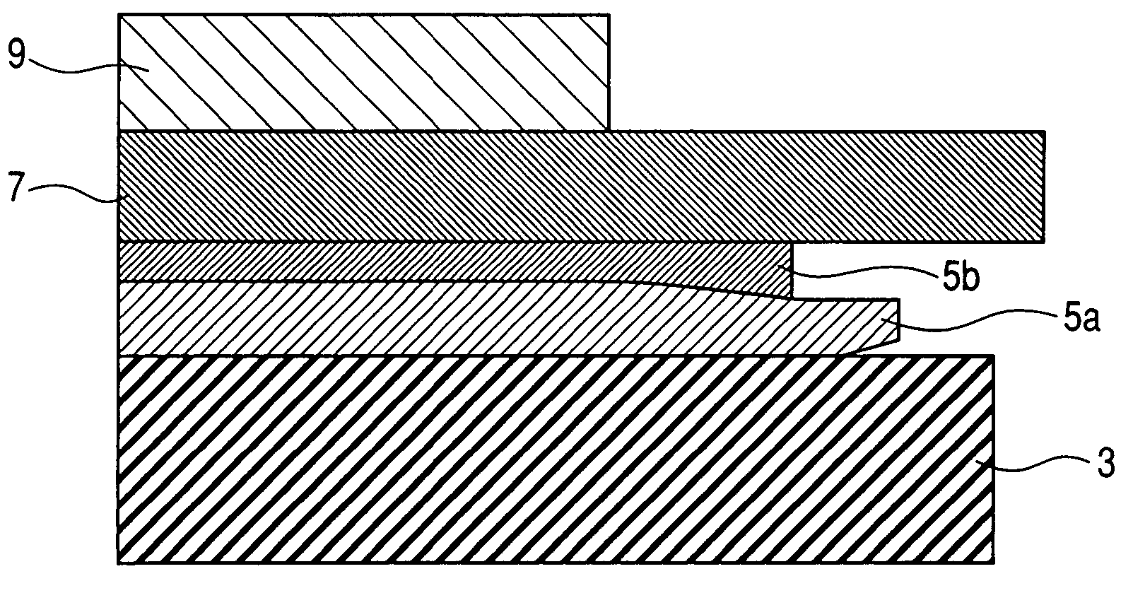
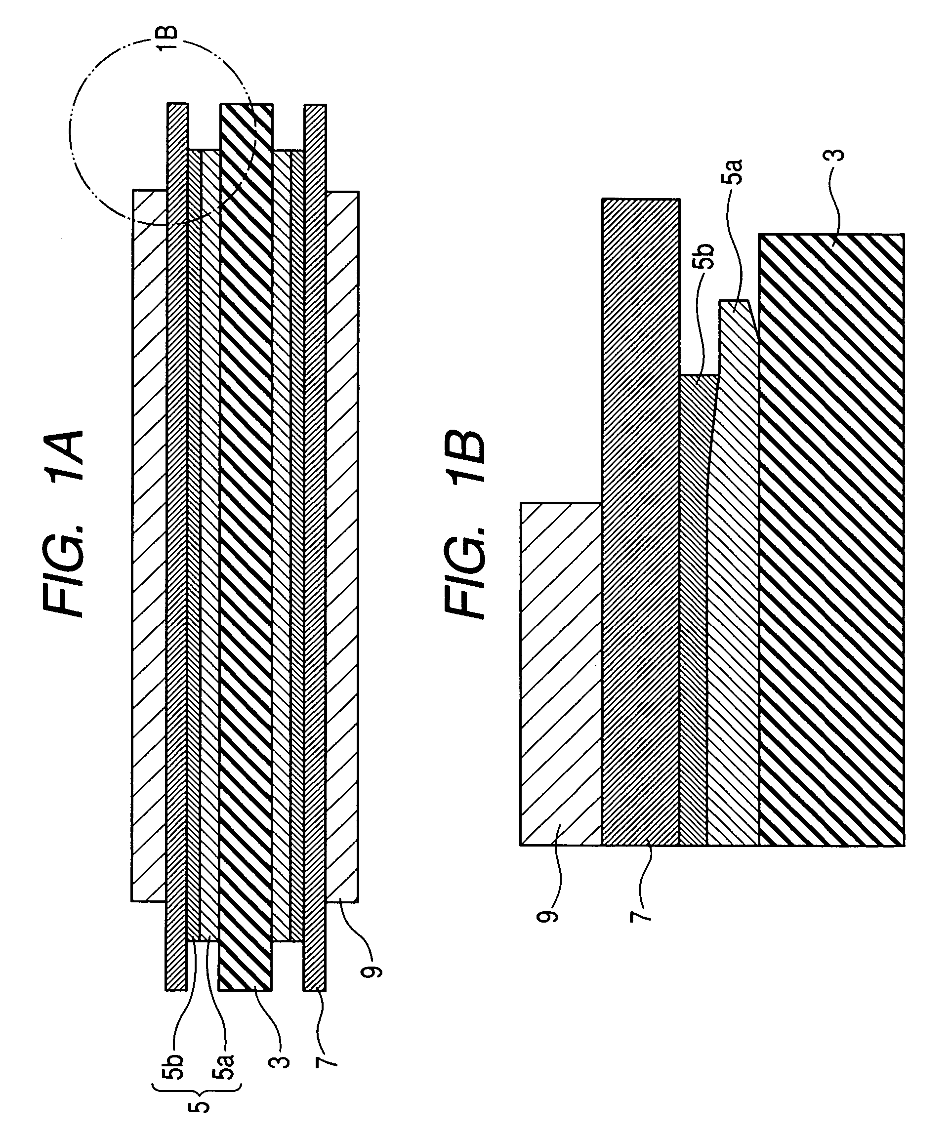
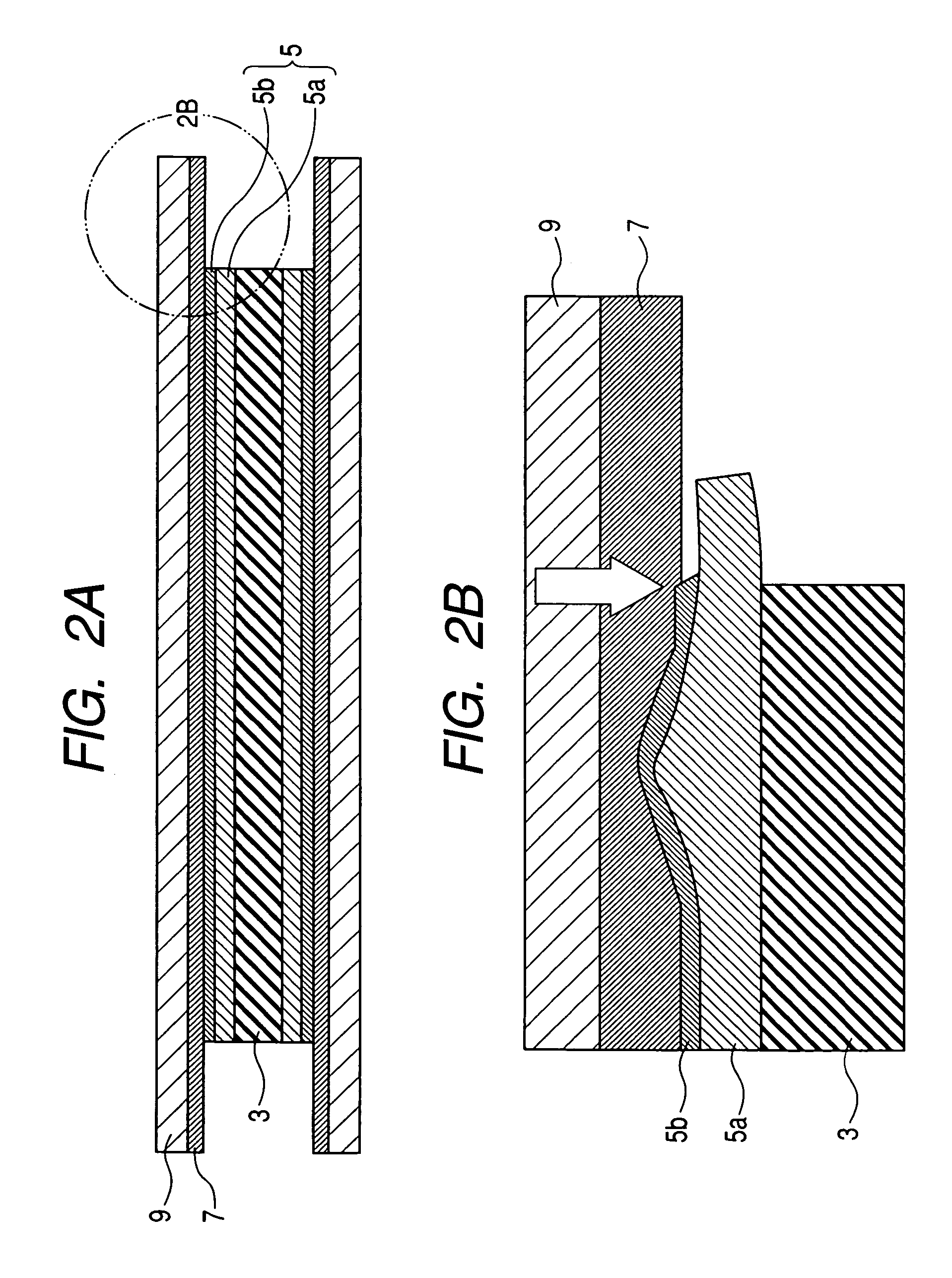
[0029]FIGS. 1A and 1B show a buffer structure in a press process according to an embodiment of the present invention, wherein the lamination state of buffer members, a substrate and RCCs etc. is shown in a cross section. FIG. 1A shows the entire structure, and FIG. 1B is an enlarged view showing a region 1B indicated in FIG. 1A. In the press process, RCCs 5, stainless steel plates 7 and buffer members 9 are laminated in the mentioned order on both surfaces of a thin plate-like substrate 3 at the center, and press plates (see FIG. 4) of a press machine are placed outside them. The RCC 5 is formed by laminating a copper foil 5b and a resin layer 5a, and it is oriented in such a way that the resin layer 5a side faces the substrate 3. The substrate 3 serves as a core substrate, the RCC 5 serves as a metal foil with resin (that is, a metal foil on which resin is at...


PUM

PropertyMeasurementUnit
heightaaaaaaaaaa
sizeaaaaaaaaaa
heightaaaaaaaaaa

Abstract

In a press process, a buffer member is placed on an RCC with a stainless steel plate between in such a way that the long sides and the short sides of the buffer member are aligned with the long sides and the short sides of the RCC respectively. The length of the long sides and the length of the short sides of the buffer member are designed to be smaller than the lengths of the long sides and the length of the short sides of the RCC respectively. With this feature, it is possible to reduce convexity on the RCC that is created in the peripheral region upon pressing the RCC to a core member.

Description

BACKGROUND OF THE INVENTION[0001]1. Field of the Invention[0002]The present invention relates to an electronic part represented by a so-called multilayer wiring substrate produced by laminating metal foils on which resin is attached on both sides of a substrate and a method of manufacturing such an electronic part. More specifically, the present invention relates to a laminated substrate having excellent surface evenness that makes it possible to apply thereon post-processing such as polishing effectively and a method of manufacturing such a laminated substrate.[0003]2. Related Background Art[0004]An electronic part called a multilayer wiring substrate was developed in order to achieve high density in electronic apparatus. In the multilayer wiring substrate, various wiring which used to be provided on a printed circuit substrate is provided inside a laminated substrate to make it possible to achieve high density mounting. In a concrete manufacturing process, wiring and electrodes et...

Claims


Application Information

Patent Timeline
Patent Type & Authority Patents(United States)
IPC IPC(8): B32B37/00
CPCB32B37/0007H05K3/4652H05K3/4611B32B37/0046B32B2457/08H05K2203/068H05K2201/0358H05K3/00H05K3/46
Inventor GOTOH, MASASHIKUWAJIMA, HAJIMEKAWABATA, KENICHI
Owner TDK CORPARATION
Why Eureka
Try Eureka