
Process for producing semiconductive porcelain composition/electrode assembly

a semi-conductive porcelain and composition technology, applied in the field of semi-conductive porcelain composition/electrode assembly production, can solve the problems of difficult application of the composition to a ptc heater, small effect of decreasing room temperature resistivity change, and high production cost, and achieve the effect of reducing the change with the passage of time and low room temperature resistivity

Inactive Publication Date: 2011-02-17
HITACHI METALS LTD
View PDF6 Cites 0 Cited by
  • Summary
  • Abstract
  • Description
  • Claims
  • Application Information

AI Technical Summary

Benefits of technology

[0013]An aspect of the present invention is to provide a semiconductive porcelain composition / electrode assembly having low room temperature resistivity of 100 Ω·cm or less and decreased change with the passage of time by enagization with regard to the semiconductive porcelain composition in which a part of Ba of BaTiO3 is substituted with Bi—Na and which has P-type semiconductive component at a crystal grain boundary.
[0016]R is at least one of rare earth elements, and is most preferably La. In the composition formula, y indicates a component range of R. When y is 0, the composition does not become conductive, whereas when y exceeds 0.02, room temperature resistivity is increased, both of which are therefore not preferred. When x and y are within the above-mentioned ranges, a semiconductive porcelain composition having smaller room temperature resistivity and excellent jump characteristic can be obtained. When the semiconductive porcelain composition having an electrode joined thereto is heat-treated at a temperature of from 100° C. to 600° C. for 0.5 hour to 24 hours, a semiconductive porcelain composition / electrode assembly having excellent change with the passage of time, low room temperature resistance of 100 Ω·cm or less, and excellent jump characteristic can be obtained.
[0018]M is at least one of Nb and Sb, and is preferably Nb. In the composition formula, z indicates a component range of M. When z is 0, valence control cannot be made and the composition does not become conductive, whereas when z exceeds 0.005, room temperature resistivity exceeds 103 Ω·cm, both of which are therefore not preferred. When x and z are within the above-mentioned ranges, a semiconductive porcelain composition having smaller room temperature resistivity and excellent jump characteristic can be obtained. When the semiconductive porcelain composition having an electrode joined thereto is heat-treated at a temperature of from 100° C. to 600° C. for 0.5 hour to 24 hours, a semiconductive porcelain composition / electrode assembly having excellent change with the passage of time, low room temperature resistance of 100 Ω·cm or less, and excellent jump characteristic can be obtained.

Problems solved by technology

As a result, the effect of decreasing room temperature resistivity change is small.
Furthermore, in the case that heat treatment temperature is lower than 100° C., it cannot make chemical equilibrium state of oxygen, whereas in the case that heat treatment is conducted at a temperature higher than 600° C., a semiconductive porcelain composition modifies due to the high temperature, room temperature resistivity becomes 100 Ω·cm or more, and it thus becomes difficult to apply the composition to a PTC heater and the like, both of which are therefore not preferred.
Furthermore, when the heat treatment time is shorter than 0.5 hour, it cannot bring close to chemical equilibrium state of oxygen, whereas when the heat treatment time exceeds 24 hours, production cost becomes too expensive, both of which are therefore not preferred.

Method used

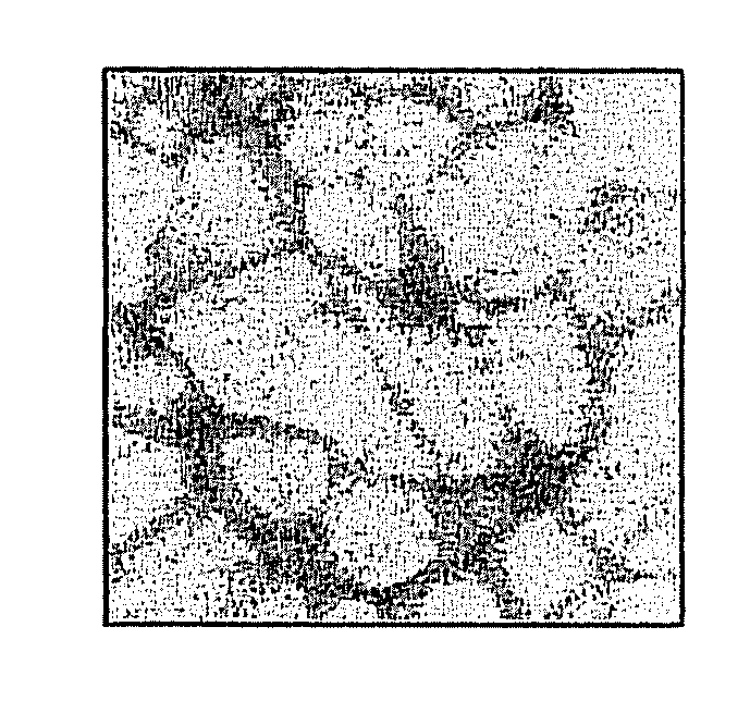
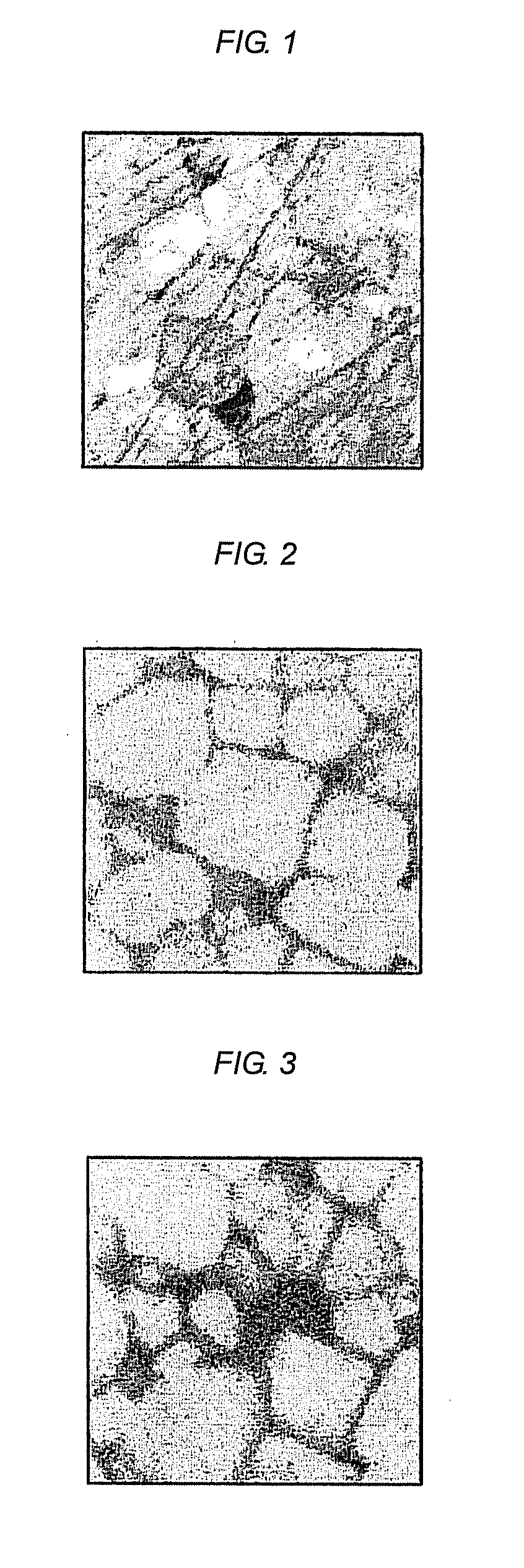
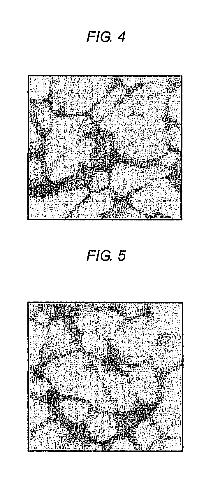

Image

  • Process for producing semiconductive porcelain composition/electrode assembly
  • Process for producing semiconductive porcelain composition/electrode assembly
  • Process for producing semiconductive porcelain composition/electrode assembly

Examples


example 1

[0064]A semiconductive porcelain composition was obtained as follows using a residual method. Raw material powders of BaCO3, TiO2 and La2O3 were prepared and blended so as to be (Ba0.994La0.006)TiO3, followed by mixing in pure water. The mixed raw material powder obtained was calcined at 900° C. for 4 hours in the air to prepare a calcined BT powder.

[0065]Raw material powders of Na2CO3, Bi2O3 and TiO2 were prepared and blended so as to be (Bi0.5Na0.5)TiO3, followed by mixing in ethanol. The mixed raw material powder obtained was calcined at 900° C. for 2 hours in the air to prepare a calcined BNT powder.

[0066]The calcined BT powder and the calcined BNT powder prepared above were blended so as to be 73 / 7 in molar ratio. The resultant was mixed and pulverized by a pot mill using pure water as a medium until a central grain size of the mixed calcined powder is from 1.0 μm to 2.0 μm, followed by drying. PVA was added to a pulverized powder of the mixed calcined powder, followed by mixin...

example 18

[0071]Raw material powders of BaCO3, TiO2 and Nb2O3 were prepared and blended so as to be Ba(Ti0.997Nb0.003)O3, followed by mixing in pure water. The mixed raw material powder obtained was calcined at 900° C. for 4 hours in the air to prepare a calcined BT powder.

[0072]Raw material powders of Na2CO3, Bi2O3 and TiO2 were prepared and blended so as to be (Bi0.5Na0.5)TiO3, followed by mixing in ethanol. The mixed raw material powder obtained was calcined at 900° C. for 2 hours in the air to prepare a calcined BNT powder.

[0073]The calcined BT powder and the calcined BNT powder, prepared above were blended so as to be 73 / 7 in molar ratio. The resulting mixture was mixed and pulverized by a pot mill using pure water as a medium until a central grain size of the mixed calcined powder is from 1.0 μm to 2.0 μm, followed by drying. PVA was added to a pulverized powder of the mixed calcined powder, followed by mixing, and the resulting mixture was granulated with a granulator. The granulated p...


PUM

PropertyMeasurementUnit
temperatureaaaaaaaaaa
Curie temperatureaaaaaaaaaa
temperatureaaaaaaaaaa

Abstract

A semiconductive porcelain composition / electrode assembly which is low in room temperature resistivity of 100 Ω·cm or less and is reduced in change with the passage of time due to energization with regard to the semiconductive porcelain composition in which a part of Ba of BaTiO3 is substituted with Bi—Na and which has a P-type semiconductive component at a crystal grain boundary. Also, there is a process for producing a semiconductive porcelain composition / electrode assembly wherein an electrode is joined to a semiconductive porcelain composition in which a part of Ba of BaTiO3 is substituted with Bi—Na and which has a P-type semiconductive component at a crystal grain boundary, the process including joining the electrode to the semiconductive porcelain composition, followed by conducting a heat treatment at a temperature of from 100° C. to 600° C. for 0.5 hour to 24 hours.

Description

CROSS-REFERENCE TO RELATED APPLICATIONS[0001]This application claims the benefit of PCT International Patent Application No. PCT / JP2009 / 054810, filed Mar. 12, 2009, and Japanese Patent Application No. 2008-082669, filed Mar. 27, 2008, in the Japanese Patent Office, the disclosures of which are incorporated herein by reference.BACKGROUND OF THE INVENTION[0002]1. Field of the Invention[0003]Aspects of the present invention relate to a process for producing a semiconductive porcelain composition / electrode assembly having a positive resistance temperature, which is used in a PTC thermistor, a PTC heater, a PTC switch, a temperature detector and the like.[0004]2. Description of the Related Art[0005]Compositions comprising BaTiO3 having added thereto various semiconductor dopants have conventionally been proposed as materials showing a PTCR characteristics (Positive Temperature Coefficient of Resistivity). Those compositions have a Curie temperature around 120° C. It is required for those...

Claims


Application Information

Patent Timeline
Patent Type & Authority Applications(United States)
IPC IPC(8): H01L21/34
CPCC01G23/003H01C7/023C01G33/006C01P2002/52C01P2004/03C01P2006/40C04B35/4682C04B35/62675C04B35/62685C04B2235/3201C04B2235/3208C04B2235/3227C04B2235/3234C04B2235/3251C04B2235/3294C04B2235/3298C04B2235/3418C04B2235/5436C04B2235/608C04B2235/656C04B2235/6567C04B2235/6584C04B2235/662C04B2235/85H01C7/02C01G29/006
Inventor INO, KENTAROSHIMADA, TAKESHI
Owner HITACHI METALS LTD
Learn More